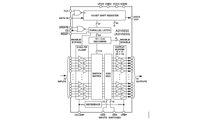
Features: ` Large, 32 * 16, nonblocking switch array
` G = +1 (ADV3202) or G = +2 (ADV3203) operation
` 32 * 32 pin-compatible version available (ADV3200/ADV3201)
`Single +5 V, dual ±2.5 V, or dual ±3.3 V supply (G = +2)
`Serial programming of switch array
`2:1 OSD insertion mux per output
`Input sync-tip clamp
`High impedance output disable allows connection of multiple devices with minimal output bus load
`Excellent video performance 60 MHz 0.1 dB gain flatness
0.1% differential gain error (RL = 150 )
0.1° differential phase error (RL = 150 )
` Excellent ac performance
Bandwidth: >300 MHz
Slew rate: >400 V/s
` Low power: 1 W
` Low all hostile crosstalk: −48 dB @ 5 MHz
` Reset pin allows disabling of all outputs
Connected through a capacitor to ground, provides power-on reset capability
` 176-lead exposed pad LQFP package (24 mm * 24 mm)
Application· CCTV surveillance
· Routing of high speed signals, including Composite video (NTSC, PAL, S, SECAM) RGB and component video routing Compressed video (MPEG, wavelet)
· Video conferencing
Pinout
 Specifications
| Parameter |
Rating |
Analog Supply Voltage (VPOS − VNEG)
Digital Supply Voltage (DVCC − DGND)
Ground Potential Difference (VNEG − DGND)
Maximum Potential Difference DVCC − VNEG
Disabled Outputs ADV3202 (|VOSD − VOUT|)
ADV3203 (|VOSD −(VOUT+VREF)/2|)
|VCLAMP − VINxx| |
7.5 V
6 V
+0.5 V to 4 V
9.4 V
<3 V
<3 V
6 V |
VREF Input Voltage ADV3202
ADV3203
Analog Input Voltage
Digital Input Voltage
Output Voltage (Disabled Analog Output)
Output Short-Circuit Duration
Output Short-Circuit Current
Storage Temperature Range
Operating Temperature Range
Lead Temperature (Soldering, 10 sec)
Junction Temperature |
VPOS 3.5 V to VNEG + 3.5 V
VPOS 4 V to VNEG + 4 V
VNEG to VPOS
DVCC
(VPOS − 1 V) to (VNEG + 1 V)
Momentary
45 mA
−65 to +125
−40 to +85
300
150 |
| Type |
32 x 16 |
| Output Buffer |
Yes G = 2 |
| Supply Voltage (V) |
±2.5V |
| Output Swing (V) |
±1.2V |
| Small Signal BW (MHz) |
300MHz |
| Slew Rate (V/us) |
400 |
| Cross Talk @ 10 MHz (-dB) |
48 dB @ 5 MHz |
| Control Interface |
Serial |
DescriptionThe ADV3202/ADV3203 are 32 * 16 analog crosspoint switch matrices. They feature a selectable sync-tip clamp input for ac-coupled applications and a 2:1 on-screen display (OSD) insertion mux. With −48 dB of crosstalk and −80 dB isolation at 5 MHz, the ADV3202/ADV3203 are useful in many high density routing applications. The 0.1 dB flatness out to 60 MHz makes the ADV3202/ADV3203 ideal for both composite and component video switching.
The 16 independent output buffers of the ADV3202/ADV3203 can be placed into a high impedance state for paralleling cross-point outputs so that off-channels present minimal loading to an output bus if building a larger array. The ADV3202 has a gain of +1 while the ADV3203 has a gain of +2 for ease of use in back-terminated load applications. A single +5 V supply, dual ±2.5 V supplies, or dual ±3.3 V supplies (G = +2) can be used while consuming only 195 mA of idle current with all outputs enabled. The channel switching is performed via a double buffered, serial digital control that can accommodate daisy chaining of several devices.
The ADV3202/ADV3203 are packaged in a 176-lead exposed pad LQFP package (24 mm* 24 mm) and are available over the extended industrial temperature range of −40 to +85.

 ADV3203 Data Sheet


