ADuC7124

DescriptionThe ADuC7124 is a fully integrated, 1 MSPS, 12-bit data acquisition system incorporating high performance multichannel ADCs, 16-bit/32-bit MCUs, and Flash/EE memory on a single chip.The ADC consists of up to 12 single-ended inputs. An additional two inputs are available but are multiple...

product image

ADuC7124 Picture
SeekIC No. : 004277877 Detail

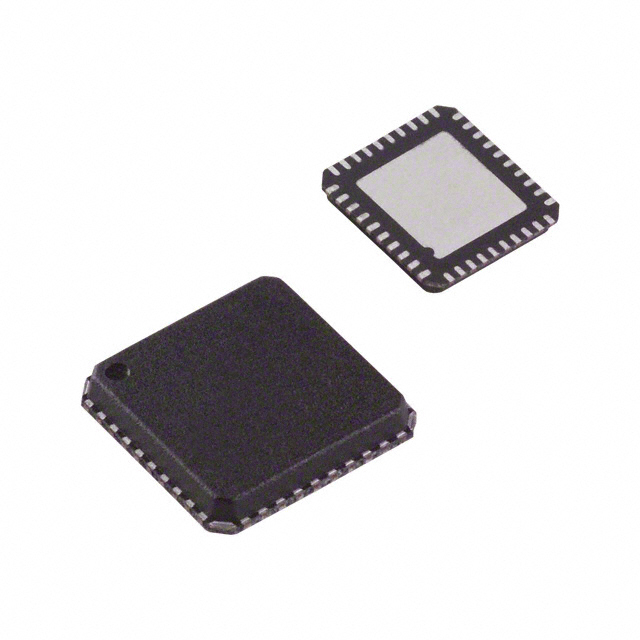
ADuC7124: DescriptionThe ADuC7124 is a fully integrated, 1 MSPS, 12-bit data acquisition system incorporating high performance multichannel ADCs, 16-bit/32-bit MCUs, and Flash/EE memory on a single chip.The A...

floor Price/Ceiling Price

Part Number:
ADuC7124
Supply Ability:
5000

Price Break

  • Qty
  • 1~5000
  • Unit Price
  • Negotiable
  • Processing time
  • 15 Days
Total Cost: $ 0.00

SeekIC Buyer Protection PLUS - newly updated for 2013!

  • Escrow Protection.
  • Guaranteed refunds.
  • Secure payments.
  • Learn more >>

Month Sales

268 Transactions

Rating

evaluate  (4.8 stars)

Upload time: 2024/4/29

Payment Methods

All payment methods are secure and covered by SeekIC Buyer Protection PLUS.

Notice: When you place an order, your payment is made to SeekIC and not to your seller. SeekIC only pays the seller after confirming you have received your order. We will also never share your payment details with your seller.
Product Details

Description


Description

The ADuC7124 is a fully integrated, 1 MSPS, 12-bit data acquisition system incorporating high performance multichannel ADCs, 16-bit/32-bit MCUs, and Flash/EE memory on a single chip.The ADC consists of up to 12 single-ended inputs. An additional two inputs are available but are multiplexed with the two DAC output pins. The ADC can operate in single-ended or differential input mode. The ADC input voltage range is 0 V to VREF. A low drift band gap reference, temperature sensor, and voltage comparator complete the ADC peripheral set.

Features of the ADuC7124 are:(1)fully differential and single-ended modes; (2)external watch crystal; (3)external clock source up to 41.78 MHz; (4)41.78 MHz PLL with programmable divider; (5)software-triggered in-circuit reprogrammability; (6)vectored interrupt controller for FIQ and IRQ; (7)8 priority levels for each interrupt type; (8)interrupt on edge or level external pin inputs.The DAC output range is programmable to one of three voltage ranges. The DAC outputs have an enhanced feature of being able to retain their output voltage during a watchdog or software reset sequence.

The absolute maximum ratings of the ADuC7124 can be summarized as:(1)AVDD to IOVDD:-0.3 V to +0.3 V;(2)storage temperature range:-65 to +150;(3)operating temperature range:-40 to +125;(4)junction temperature:+150;(5)AGND to DGND:-0.3V to +0.3V;(6)digital input voltage to IOGND:-0.3 V to +5.3 V.Stresses above those listed under Absolute Maximum Ratings may cause permanent damage to the device. This is a stress rating only; functional operation of the device at these or any other conditions above those indicated in the operational section of this specification is not implied.Exposure to absolute maximum rating conditions for extended periods may affect device reliability.The access time reading or writing a MMR depends on the advanced microcontroller bus architecture (AMBA) bus used to access the peripheral. The processor has two AMBA buses:the advanced high performance bus (AHB) used for system modules, and the advanced peripheral bus (APB) used for the lower performance peripheral. Access to the AHB is one cycle,and access to the APB is two cycles. All peripherals on the ADuC7124 are on the APB except the Flash/EE memory and the GPIOs.


Customers Who Bought This Item Also Bought

Margin,quality,low-cost products with low minimum orders. Secure your online payments with SeekIC Buyer Protection.
Cables, Wires - Management
Batteries, Chargers, Holders
Inductors, Coils, Chokes
RF and RFID
Tapes, Adhesives
803
Test Equipment
View more