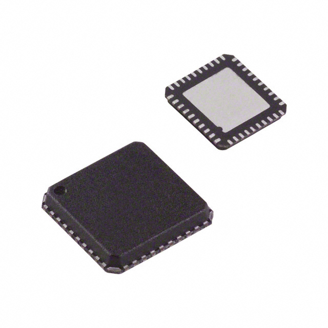
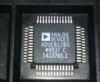
DescriptionThe ADuC7128 is fully integrated, 1 MSPS, 12-bit data acquisition system incorporating a high performance, multichannel analog-to-digital converter (ADC), DDS with line driver, 16-/32-bit MCU, and Flash/EE memory on a single chip.The ADC consists of up to 14 single-ended inputs. The ADC can operate in single-ended or differential input modes. The ADC input voltage is 0 to VREF. Low drift band gap reference,temperature sensor, and voltage comparator complete the ADC peripheral set.
Features of the ADuC7128 are:(1)up to 14 analog-to-digital converter (ADC) channels; (2)fully differential and single-ended modes; (3)0 to VREF analog input range; (4)ARM7TDMI core, 16-/32-bit RISC architecture; (5)JTAG port supports code download and debug; (6)external watch crystal/clock source; (7)in-circuit download, JTAG-based debug; (8)software triggered in-circuit reprogrammability.The devices operate from an on-chip oscillator and PLL, generating an internal high frequency clock of 41.78 MHz. This clock is routed through a programmable clock divider from which the MCU core clock operating frequency is generated.
The absolute maximum ratings of the ADuC7128 can be summarized as:(1)AVDD to DVDD:-0.3V to +6.0V;(2)storage temperature range:-65 to +150;(3)AGND to DGND:-0.3 V to +0.3 V;(4)junction temperature:+150;(5)IOVDD to IOGND, AVDD to AGND:-0.3 V to +6 V.Stresses above those listed under Absolute Maximum Ratings may cause permanent damage to the device. This is a stress rating only; functional operation of the device at these or any other conditions above those indicated in the operational section of this specification is not implied.Exposure to absolute maximum rating conditions for extended periods may affect device reliability.An ARM® instruction is 32-bits long. The ADuC7128 processor supports a second instruction set that has been compressed into 16-bits, called the Thumb instruction set. Faster execution from 16-bit memory and greater code density can usually be achieved by using the Thumb instruction set instead of the ARM instruction set, which makes the ADuC7128 core particularly suitable for embedded applications.

 ADuC7128 Data Sheet