ALD1712A

Features: • Linear mode operation with input voltages 300mV beyond supply rails• Symmetrical complementary output drive• Output voltages to within 2mV of power supply rails• High load capacitance capability -- 4000pF typical• No frequency compensation required -- unit...

product image

ALD1712A Picture
SeekIC No. : 004279772 Detail

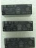
ALD1712A: Features: • Linear mode operation with input voltages 300mV beyond supply rails• Symmetrical complementary output drive• Output voltages to within 2mV of power supply rails• ...

floor Price/Ceiling Price

Part Number:
ALD1712A
Supply Ability:
5000

Price Break

  • Qty
  • 1~5000
  • Unit Price
  • Negotiable
  • Processing time
  • 15 Days
Total Cost: $ 0.00

SeekIC Buyer Protection PLUS - newly updated for 2013!

  • Escrow Protection.
  • Guaranteed refunds.
  • Secure payments.
  • Learn more >>

Month Sales

268 Transactions

Rating

evaluate  (4.8 stars)

Upload time: 2024/4/29

Payment Methods

All payment methods are secure and covered by SeekIC Buyer Protection PLUS.

Notice: When you place an order, your payment is made to SeekIC and not to your seller. SeekIC only pays the seller after confirming you have received your order. We will also never share your payment details with your seller.
Product Details

Description


Features:

• Linear mode operation with input voltages 300mV beyond supply rails
• Symmetrical complementary output drive
• Output voltages to within 2mV of power supply rails
• High load capacitance capability -- 4000pF typical
• No frequency compensation required -- unity gain stable
• Extremely low input bias currents -- 0.01pA typical
• Dual power supply ±2.5V to ±6.0V
• Single power supply +5V to +12V
• High voltage gain typically 85V/mV @ ±2.5V and 250V/mV @ ±5.0V
• Drive as low as 1KW load with 5mA drive current
• Output short circuit protected
• Unity gain bandwidth of 1.5MHz
• Slew rate of 2.1V/ms


Application

• Voltage amplifier
• Voltage follower/buffer
• Charge integrator
• Photodiode amplifier
• Data acquisition systems
• High performance portable instruments
• Signal conditioning circuits
• Sensor and transducer amplifiers
• Low leakage amplifiers
• Active filters
• Sample/Hold amplifier
• Picoammeter
• Current to voltage converter
• Coaxial cable driver


Specifications

Supply voltage, V+                                                                  13.2V
Differential input voltage range                                               -0.3V to V+ +0.3V
Power dissipation                                                                    600 mW
Operating temperature range PA,SA package                         0°C to +70°C
                                                     DA package                        -55°C to +125°C
Storage temperature range                                                   -65°C to +150°C
Lead temperature, 10 seconds                                               +260°C


Description

The ALD1712 is a monolithic precision operational amplifier intended primarily for a wide range of analog applications in +5V single power supply and ±5V dual power supply systems as well as +6V to 12V battery operated systems. All device characteristics are specified for +5V single supply or ±2.5V dual supply systems. ALD1712 is manufactured with Advanced Linear Devices' enhanced ACMOS silicon gate CMOS process and is available as a standard cell in ALD's ASIC "Function-Specific" library.

The ALD1712 has an input stage that operates to +300mV above and -300mV below the supply voltages with no adverse effects and/or phase reversals.

The ALD1712 has been developed specifically with the 5V single supply or ±2.5V dual supply user in mind. Several important characteristics of the device make many applications easy to implement for these supply voltages. First, the operational amplifier can operate with rail-to-rail input and output voltages. This feature allows numerous analog serial stages to be implemented without losing operating voltage margin. Secondly, the ALD1712 was designed to accommodate mixed applications where digital and analog circuits may work off the same 5V power supply. Thirdly, the output stage can drive up to 400pF capacitive, and 1KW resistive loads in non-inverting unity gain connection, and up to 4000pF at a gain of 5. These features, coupled with extremely low input currents, high voltage gain,
useful bandwidth of 1.5MHz, slew rate of 2.1V/ms, low power dissipation, low offset voltage and temperature drift, make the ALD1712 a truly versatile, user friendly, operational amplifier.

On-chip offset voltage trimming allows the device to be used without nulling in most applications. The ALD1712 offers typical offset drift of less than 5mV/ °C which eliminates many trim or temperature compensation circuits. For precision applications, the 1712 is designed to settle to 0.01% in 8ms. The unique characteristics at input and output are modeled in an available macromodel.


Customers Who Bought This Item Also Bought

Margin,quality,low-cost products with low minimum orders. Secure your online payments with SeekIC Buyer Protection.
Undefined Category
Optical Inspection Equipment
Prototyping Products
DE1
Semiconductor Modules
Circuit Protection
View more