AS29F010

Features: • Organization: 128K × 8 bits• Sector Erase architecture- Four 32K × 8 sectors• Single 5.0±0.5V power supply for read/write operations• High speed 120/150 ns address access time• Low power consumption:- 30 mA maximum read current- 50 mA maximum program curre...

product image

AS29F010 Picture
SeekIC No. : 004288274 Detail

AS29F010: Features: • Organization: 128K × 8 bits• Sector Erase architecture- Four 32K × 8 sectors• Single 5.0±0.5V power supply for read/write operations• High speed 120/150 ns addres...

floor Price/Ceiling Price

Part Number:
AS29F010
Supply Ability:
5000

Price Break

  • Qty
  • 1~5000
  • Unit Price
  • Negotiable
  • Processing time
  • 15 Days
Total Cost: $ 0.00

SeekIC Buyer Protection PLUS - newly updated for 2013!

  • Escrow Protection.
  • Guaranteed refunds.
  • Secure payments.
  • Learn more >>

Month Sales

268 Transactions

Rating

evaluate  (4.8 stars)

Upload time: 2024/4/17

Payment Methods

All payment methods are secure and covered by SeekIC Buyer Protection PLUS.

Notice: When you place an order, your payment is made to SeekIC and not to your seller. SeekIC only pays the seller after confirming you have received your order. We will also never share your payment details with your seller.
Product Details

Description


Features:

• Organization: 128K × 8 bits
• Sector Erase architecture
- Four 32K × 8 sectors
• Single 5.0±0.5V power supply for read/write operations
• High speed 120/150 ns address access time
• Low power consumption:
- 30 mA maximum read current
- 50 mA maximum program current
- 1.5 mA maximum standby current
- 1 mA maximum standby current (low power)
• 10,000 write/erase cycle endurance
• JEDEC standard write cycle commands
- protects data from accidental changes
• Program/erase cycle end signals:
-Data polling
- DQ6 toggle
• Low VCC write lock-out below 3.2V
• JEDEC standard packages and pinouts:
-32-pin DIP
- 32-pin PLCC
- 32-pin TSOP


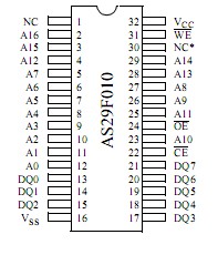
Pinout

  Connection Diagram


Specifications

Parameter Symbol Min Max Unit
Input voltage (Input or DQ pin) VIN 1.0 VCC + 1.0 V
Input voltage (A9 pin) VIN 1.0 +13.0 V
Output voltage VOUT 1.0 VCC + 1.0 V
Power supply voltage VCC +4.5 +5.5 V
Operating temperature TOPR 55 +125 °C
Storage temperature (plastic) TSTG 65 +125 °C
Short circuit output current IOUT - 100 mA
Latch-up current IIN - ±100 mA


Description

The AS29F010 is a high performance 1 megabit 5 volt-only Flash memory organized as 128K bytes of 8 bits each. AS29F010 is divided into four sectors of 32K bytes each. Each sector is separately erased and programmed without affecting data in the other sectors. All program, erase, and verify operations are 5-volt only, and require no external 12V supply pin. All required features for in-system programmability are provided.

The AS29F010 provides high performance with a maximum access time of 120, or 150 ns. Chip Enable ( CE), Output Enable (OE), and Write Enable (WE) pins allow easy interface with the system bus.

Program, erase, and verify operations of AS29F010 are controlled with an on-chip command register using a JEDEC standard Write State Machine approach to enter commands. Each command requires four write cycles to be executed. Address and data are latched internally during all write, erase, and verify operations, and an internal timer terminates each command. The AS29F010 has a typical timer period of 200 µs for all commands but Erase, which has a typical period of 800 ms. Under nominal conditions, a sector can be completely programmed and ver i fied in less than 12 seconds. To program, erase, and verify a sector typically takes less than 18 seconds.

Data protection of AS29F010 is provided by a low-VCC lockout and by error checking in the Write State Machine.DATA polling and Toggle Bit modes are used to show that the chip is executing a command when the AS29F010 is read during a write or erase operation. After Erase or P ogram commands, Verify-1 and Verify-0 command modes ensure sufficient margin for reliable operation. (See command summary on page 5.)

The AS29F010 is packaged in 32-pin DIP, PLCC and TSOP packages with JEDEC standard pinouts for one megabit Flash memories.


Customers Who Bought This Item Also Bought

Margin,quality,low-cost products with low minimum orders. Secure your online payments with SeekIC Buyer Protection.
Inductors, Coils, Chokes
Programmers, Development Systems
Memory Cards, Modules
Soldering, Desoldering, Rework Products
Prototyping Products
DE1
Sensors, Transducers
View more