Features: • Organization
- 1,048,576 words × 8 bits × 2 banks (2M × 8) 11 row, 9 column address
- 524,288 words × 16 bits × 2 banks (1M × 16) 11 row, 8 column address
• All signals referenced to positive edge of clock, fully synchronous
• Dual internal banks controlled by A11 (bank select)
• High speed
- 143/125/100 MHz
- 7/8/10 ns clock access time
• Low power consumption
- Active: 576 mW max
- Standby: 7.2 mW max, CMOS I/O
• 2048 refresh cycles, 32 ms refresh interval
• 4096 refresh cycles, 64 ms refresh interval
• Auto refresh and self refresh
• PC100 functionality
• Automatic and direct precharge including concurrent autoprecharge
• Burst read, write/Single write
• Random column address assertion in every cycle, pipelined operation
• LVTTL compatible I/O
• 3.3V power supply
• JEDEC standard package, pinout and function
- 400 mil, 44-pin TSOP 2 (2M × 8)
- 400 mil, 50-pin TSOP 2 (1M × 16)
• Read/write data masking
• Programmable burst length (1/2/4/8/ full page)
• Programmable burst sequence (sequential/interleaved)
• Programmable CAS latency (1/2/3)Pinout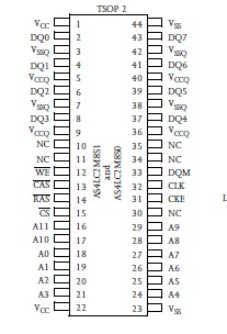 Specifications
|
Parameter |
Symbol |
Min |
Max |
Unit |
Notes |
|
Input voltage
Power supply voltage
Storage temperature (plastic)
Power dissipation
Short circuit output current |
V IN,V OUT
V CC,V CCQ
T STG
P D
IOUT |
1.0
1.0
55
|
+4.6
+4.6
+150
1
50 |
V
V
°C
W
mA |
|
Note: Stresses greater than those listed under Absolute Maximum Ratings may cause permanent damage to the device. This is a stress rating only and functional operation of the device at these or any other conditions outside those indicated in the operational sections of this specification is not implied. Exposure to absolute maximum rating conditions for extended periods may affect reliability.
DescriptionThe AS4LC2M8S1, AS4LC2M8S0, and AS4LC1M16S1, AS4LC1M16S0 are high-performance 16-megabit CMOS Synchronous Dynamic Random Access Memory (SDRAM) devices organized as 1,048,576 words × 8 bits × 2 banks (2048 rows × 512 columns) and 524,288 words × 16 bits × 2 banks (2048 rows × 256 columns), respectively. Very high bandwidth is achieved using a pipelined architecture where all inputs and outputs are referenced to the rising edge of a common clock. Programmable burst mode of AS4LC2M8S0 can be used to read up to a full page of data (512 bytes for 2M × 8 and 256 bytes for 1M × 16) without selecting a new column address.
The operational advantages of an SDRAM AS4LC2M8S0 are as follows: (1) the ability to synchronously output data at a high clock frequency with automatic increments of column-address (burst access); (2) bank-interleaving, which hides precharge time and attains seamless operation; and (3) the capability to change column-address randomly on every clock cycle during burst access.
This SDRAM product also features of AS4LC2M8S0 a programmable mode register, allowing users to select read latency as well as burst length and type (sequential or interleaved). Lower latency improves first data access in terms of CLK cycles, while higher latency improves maximum frequency of operation. This feature of AS4LC2M8S0 enables flexible performance optimization for a variety of applications.
SDRAM commands and functions of AS4LC2M8S0 are decoded from control inputs. Basic commands are as follows:
• Mode register set • Deactivate bank • Deactivate all banks • Select row; activate bank
• Select column; write • Select column; read • Deselect; power down • CBR refresh
• Auto precharge with read/write • Self-refresh
Both devices are available in 400-mil plastic TSOP type 2 package. The AS4LC2M8S1/ AS4LC2M8S0 have 44 pins, and the AS4LC1M16S1/ AS4LC1M16S0 have 50 pins. AS4LC2M8S0 operate with a power supply of 3.3V ± 0.3V. Multiple power and ground pins are provided for low switching noise and EMI. Inputs and outputs are LVTTL compatible.

 AS4LC2M8S0 Data Sheet