Features: ` AS7C1026(5V version)
` AS7C31026(3.3V version)
` Industrial and commercial temperatures
` Organization: 655,36 words x 16 bits
`High speed
- 10/12/15/20 ns address access time
- 5, 6, 7, 8 ns output enable access time
` Low power consumption: ACTIVE
- 880 mW (AS7C1026) / max @ 12ns
- 396 mW (AS7C31026) / max @ 12 ns
` Low power consumption: STANDBY
- 28 mW (AS7C1026A) / max CMOS
- 18 mW (AS7C31026) / max CMOS
` 2.0V data retention
` Easy memory expansion with CE , OE inputs
` TTL/LVTTL-compatible, three-state I/O
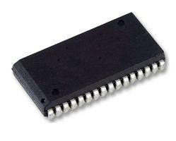
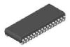
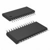
` JEDEC standard packaging
- 44-pin 400 mil SOJ
- 44-pin 400 mil TSOP II
- 48-ball 6 mm * 8 mm CSP mBGA
` ESD protection 2000 volts
`Latch-up current 200 mAPinout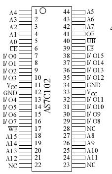 Specifications
| Parameter |
Symbol |
Min |
Max |
Unit |
| Voltage on VCC relative to GND |
AS7C1026 |
Vt1 |
-0.50 |
+7.0 |
V |
| AS7C31026 |
Vt1 |
0.50 |
+5.0 |
V |
| Voltage on any I/O pin relative to GND |
Both |
Vt2 |
0.50 |
VCC+ 0.50 |
V |
| Power dissipation |
Both |
PD |
|
1.0 |
W |
| Storage temperature (plastic) |
Both |
Tstg |
65 |
+150 |
|
Temperature with VCC applied
|
Both |
Tbias |
55 |
+125 |
|
| DC output current (low) |
Both |
IOUT |
|
20 |
mA |
DescriptionThe AS7C1026 and AS7C31026 are high-performance CMOS 1,048,576-bit Static Random Access Memory (SRAM) devices organized as 65,536 words x 16 bits. They are designed for memory applications where fast data access, low power, and simple interfacing are desired.
Equal address access and cycle times (tAA, tRC, tWC) of 10/12/15/20 ns with output of AS7C31026 enable access times (tOE) of 5/6/8/10 ns are ideal for high-performance applications.
When CE is high AS7C31026 enter stanby mode. The AS7C1026 is guaranteed not to exceed 28 mW power consumption in CMOS standby mode. The devices also offer 2.0V data retention.
A write cycle of AS7C31026 is accomplished by asserting write enable (WE ) and chip enable (CE). Data on the input pins I/O0I/O15 is written on the rising edge of WE (write cycle 1) or CE (write cycle 2). To avoid bus contention, external devices should drive I/O pins only after outputs have been disabled with output enable (OE ) or write enable (WE ).
A read cycle of AS7C31026 is accomplished by asserting output enable (OE ) and chip enable (CE), with write enable (WE ) high. the chips drive I/O pins with the data word referenced by the input address. When either chip enable or output enable is inactive, or write enable is active, output drivers stay in high-impedance mode.
AS7C31026 provide multiple center power and ground pins, and separate byte enable controls, allowing individual bytes to be written and read. LB controls the lower bits, I/O0I/O7, and UB controls the higher bits, I/O8I/O15.
All chip inputs and outputs are TTL-compatible, and operation is from a single 5V supply (AS7C1026) or 3.3V supply (AS7C31026). the device is packaged in common industry standard packages. Chip scale BGA packaging, easy to use in manufacturing, provides the smallest possible footprint. This 48-ball JEDEC-registered package has a ball pitch of 0.75 mm and
external dimensions of 8 mm * 6 mm.

 AS7C31026 Data Sheet