AS80M2516A

Features: ` Two on chip PLLs. ` Generates an EMI optimized clocking signal at output. ` Non Spread spectrum mode available ` Input Frequency Range 2MHz 200Mhz in Non Spread mode ` Input Frequency Range 6Mhz 80Mhz in Spread mode. ` Output Frequency Range 4Mhz 140Mhz. ` Four frequency outputs; two...

product image

AS80M2516A Picture
SeekIC No. : 004288590 Detail

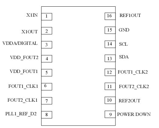
AS80M2516A: Features: ` Two on chip PLLs. ` Generates an EMI optimized clocking signal at output. ` Non Spread spectrum mode available ` Input Frequency Range 2MHz 200Mhz in Non Spread mode ` Input Frequency Ra...

floor Price/Ceiling Price
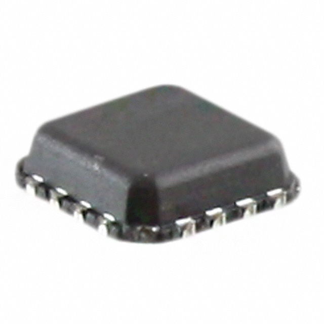
Part Number:
AS80M2516A
Supply Ability:
5000

Price Break

  • Qty
  • 1~5000
  • Unit Price
  • Negotiable
  • Processing time
  • 15 Days
Total Cost: $ 0.00

SeekIC Buyer Protection PLUS - newly updated for 2013!

  • Escrow Protection.
  • Guaranteed refunds.
  • Secure payments.
  • Learn more >>

Month Sales

268 Transactions

Rating

evaluate  (4.8 stars)

Upload time: 2024/4/27

Payment Methods

All payment methods are secure and covered by SeekIC Buyer Protection PLUS.

Notice: When you place an order, your payment is made to SeekIC and not to your seller. SeekIC only pays the seller after confirming you have received your order. We will also never share your payment details with your seller.
Product Details

Description


Features:

`    Two on chip PLLs.  
`    Generates an EMI optimized clocking signal at output.
`    Non Spread spectrum mode available
`    Input Frequency Range 2MHz 200Mhz in Non Spread mode 
`    Input Frequency Range 6Mhz 80Mhz in Spread mode.
`    Output Frequency Range 4Mhz 140Mhz.
`    Four frequency outputs; two per PLL. 
`    Programmable spread  range and type of modulation ( center or down) and type of profile.
`    Power down feature is incorporated.
`    Both the PLL have reference frequency output.
`    Supply voltage range 3.3 V (± 0.3) 
`    Software is available for configuring  all the parameters of the Chip,  through I2C . 


Pinout

  Connection Diagram


Specifications

PARAMETER SYMBOL MIN MAX UNITS
Supply Voltage, dc (Vss = ground) VDD VSS-0.5 7 V
Input Voltage, dc  VI  VSS-0.5  VDD+0.5 V
Output Voltage, dc VO VSS-0.5 VDD+0.5 V
Input Clamp Current, dc (VI < 0 or VI >VDD) IIK -50 50 mA
Output Clamp Current, dc (VI < 0 or VI >VDD) IOK -50 50 mA
Storage Temperature Range (non condensing) TS -65 150 °C
Ambient Temperature Range, Under Bias TA -55 125 °C
Junction Temperature TJ   150 °C
Lead Temperature (soldering, 10s)     260 °C
Input Static Discharge Voltage Protection (MIL STD 883E, Method 3015.7)     2 kV


Description

The AS80M2516A is dual phase lock loop clock chip. That is a versatile spread spectrum frequency modulator design specifically for a wide range of clock frequencies. 


The AS80M2516A reduces electromagnetic interference (EMI) at clock source. That allows significant system cost savings by reducing the number of circuit board layers and shielding that are required to pass EMI regulations.


The AS80M2516A is I2C configurable. All the functional parameters of it can be configured from external I2C master unit through I2C bus.
 
The AS80M2516A modulates the output of PLL in order to spread the bandwidth of a synthesized clock , there by decreasing the peak amplitudes of its harmonics. This results in significantly lower system EMI compared to the typical narrow band signal  of AS80M1800 produced by oscillator and most clock generators. Lowering EMI by increasing a signal's bandwidth is called spread spectrum clock generation.


Customers Who Bought This Item Also Bought

Margin,quality,low-cost products with low minimum orders. Secure your online payments with SeekIC Buyer Protection.
LED Products
Inductors, Coils, Chokes
Circuit Protection
Motors, Solenoids, Driver Boards/Modules
Computers, Office - Components, Accessories
View more