Features: ` Differential clock signals
`Meets SSTL_2 class II specifications on outputs
` Low voltage operation VDD = 2.3 V to 2.7 V
` Available in 64-pin TSSOP and 56-pin VFQFN packages (MLF2)Application· DDR memory modules: PC1600, PC2100, PC2700, AND PC3200
· Provides complete DDR DIMM logic solution with PCV857
· SSTL_2-compatible data registersPinout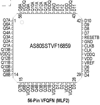 Specifications
| Storage temperature |
- 65° C to +150° C |
| Supply voltage |
-0.5 to 3.6 V |
Input voltage1 |
-0.5 to VDD + 0.5
|
Output voltage1,2 |
-0.5 to VDD + 0.5
|
| Input clamp current |
± 50 mA |
| Output clamp current |
± 50 mA |
| Continuous output current |
± 50 mA |
VDD , VDDQ , or GND current/pin
|
± 100 mA |
Package thermal impedance3 |
55° C/W |
DescriptionThe 13-bit to 26-bit PC16859 is a universal bus driver designed for 2.3 V to 2.7 V VDD operation and SSTL_2 I/O levels, except for the LVCMOS RESETB input.
Data flow from D to Q is controlled by the differential clock (CLK/CLKB) and a control signal (RESETB). The positive edge of CLK is used to trigger the data flow, and CLKB is used to maintain sufficient noise margins, whereas RESETB, an LVCMOS asynchronous signal, is intended for use only at power-up. PC16859 supports low-power standby operation. A logic level low at RESETB assures that all internal registers and outputs (Q) are reset to the logic low state, and that all input receivers, data (D), and clock (CLK/CLKB) are switched off. Note that RESETB must always be supported with LVCMOS levels at a valid logic state because VREF may not be stable during power-up.
To ensure that outputs are at a defined logic state before a stable clock has been supplied, RESETB must be held at a logic low level during power-up.
In the DDR DIMM application, RESETB is specified to be completely asynchronous with respect to CLK and CLKB, therefore, no timing relationship can be guaranteed between the two signals. When entering a low-power standby state, the register will be cleared and the outputs will be driven to a logic low level quickly relative to the time to disable the differential input receivers. This ensures there are no glitches on the output. When coming out of low power standby state, however, the register will become active quickly relative to the time to enable the differential input receivers. When the data inputs are at a logic level low and the clock is stable during the low-to-high transition of RESETB until the input receivers are fully enabled, the design ensures that the outputs will remain at a logic low level.

 AS80SSTVF16859 Data Sheet