Features: · Patented on-chip Phase-Locked Loop with VCO for
clock generation
· Provides reference clock and synthesized clock
· Generates frequencies from 2 to 120 MHz (depending
on option), operates to 80 MHz for VDD 3.3V±10%
· 8-pin DIP or SOIC package or 14-pin DIP or SOIC package
· 2 to 32 MHz input reference frequency (depending on option)
· On-chip loop filter
· Up to 16 frequencies stored internally
· Low power CMOS technology
· Single +3.3 or +5 volt power supplyApplicationGraphics: The AV9107C is the easiest to use, lowest cost, and smallest footprint frequency generator for graphics applications. It can generate up to 16 different frequencies, including all frequencies necessary for VGA standards. It should be used in place of the AV9105/6 when the reference clock is also needed.
Computer: The AV9107C is the ideal solution for replacing high speed oscillators and for reducing clock speeds to save power in computers. The device provides smooth, glitchfree frequency transitions so that the CPU can continue to operate during slow down or speed up. The rate of frequency change makes the AV9107C compatible with all 386DX, 386SX, 486DX, 486DX2, and 486SX devices. Standard versions include the AV9107C-03, -05, -10, -11. Disk Drives: Smaller than a single crystal or an oscillator, the tiny SOIC package can be used for any general purpose frequency generation in disk drives.
Pinout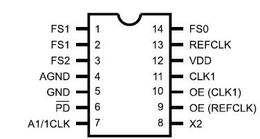 SpecificationsAVDD, VDD referenced to GND ...................................................................................................................................... 7V
Operating temperature under bias .............................................................................................................. 0°C to +70°C
Storage temperature ............................................................................................................................. -65°C to +150°C
Voltage on I/O pins referenced to GND ....................................................................................... GND -0.5V to VDD +0.5V
Power dissipation ......................................................................................................................................................... 0.5 Watts
Stresses above those listed under Absolute Maximum Ratings may cause permanent damage to the device. This is a stress rating
only and functional operation of the device at these or any other conditions above those indicated in the operational sections of
the specifications is not implied. Exposure to absolute maximum rating conditions for extended periods may affect product
reliability.DescriptionThe AV9107C offers a tiny footprint solution for generating two simultaneous clocks. One clock, the REFCLK, is a fixed output frequency which is the same as the input reference crystal (or clock). The other clock, CLK1, can vary between 2 and 120 MHz, with up to 16 selectable preprogrammed frequencies stored in internal ROM (frequency range depends on design option).
The AV9107C has advanced features which include on-chip loop filters, tristate outputs, and power-down capability. A minimum of external components - two decoupling capacitors and an optional ferrite bead - are all that are required for jitter-free operation. Standard versions for computer motherboard applications are the AV9107C-03, and AV9107C-05. Custom masked versions, with customized frequencies and features, are available in 6-8 weeks for a small NRE.

 AV9107C Data Sheet