Am79514

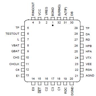
PinoutSpecificationsStorage temperature ..................................55 to +150 VCC with respect to AGND/DGND .................0.4 V to +7.0 VVEE with respect to AGND/DGND...................+0.4 V to 7.0 VVBAT with respect to AGND/DGND................. +0.4 V to 70 VNote: Rise time of VBAT (d...

product image

Am79514 Picture
SeekIC No. : 004284342 Detail

Am79514: PinoutSpecificationsStorage temperature ..................................55 to +150 VCC with respect to AGND/DGND .................0.4 V to +7.0 VVEE with respect to AGND/DGND...................+0....

floor Price/Ceiling Price

Part Number:
Am79514
Supply Ability:
5000

Price Break

  • Qty
  • 1~5000
  • Unit Price
  • Negotiable
  • Processing time
  • 15 Days
Total Cost: $ 0.00

SeekIC Buyer Protection PLUS - newly updated for 2013!

  • Escrow Protection.
  • Guaranteed refunds.
  • Secure payments.
  • Learn more >>

Month Sales

268 Transactions

Rating

evaluate  (4.8 stars)

Upload time: 2024/4/18

Payment Methods

All payment methods are secure and covered by SeekIC Buyer Protection PLUS.

Notice: When you place an order, your payment is made to SeekIC and not to your seller. SeekIC only pays the seller after confirming you have received your order. We will also never share your payment details with your seller.
Product Details

Description


Pinout

  Connection Diagram


Specifications

Storage temperature ..................................55  to +150
VCC with respect to AGND/DGND .................0.4 V to +7.0 V
VEE with respect to AGND/DGND...................+0.4 V to 7.0 V
VBAT with respect to AGND/DGND................. +0.4 V to 70 V
Note: Rise time of VBAT (dv/dt) must be limited to 27 V/s or
less when QBAT bypass = 0.33 F.
BGND with respect to AGND/DGND.............. +1.0 V to 3.0 V
A(TIP) or B(RING) to BGND:
Continuous ................................................. 70 V to +1.0 V
10 ms (f = 0.1 Hz) ....................................... 70 V to +5.0 V
1 s (f = 0.1 Hz) ........................................... 90 V to +10 V
250 ns (f = 0.1 Hz) ..................................... 120 V to +15 V
Current from A(TIP) or B(RING)............................... ±150 mA
Voltage on RINGOUT .................... BGND to 70 V above QBAT
Voltage on TESTOUT ....... .............BGND to 70 V above QBAT
Current through relay drivers ......................................60 mA
Voltage on ring-trip inputs DA and DB .................VBAT to 0 V
Current into ring-trip inputs.................................. ...±10 mA
Peak current into regulator switch (L pin) .................150 mA
Switcher transient peak off voltage on L pin ..............+1.0 V
C4C1, E1, CHCLK,
to AGND/DGND....................................0.4 V to VCC + 0.4 V
Maximum power dissipation, (see note) ................TA = 70
In 32-pin PLCC package.............................................1.74 W

Note: Thermal limiting circuitry on chip will shut down the circuit at a junction temperature of about 165 . The device
should never be exposed to this temperature. Operation above 145 junction temperature may degrade device
reliability. See the SLIC Packaging Considerations for more information.

Stresses above those listed under Absolute Maximum Ratings may cause permanent device failure. Functionality at or above these limits is not implied. Exposure to Absolute Maximum Ratings for extended periods may affect device reliability.


Customers Who Bought This Item Also Bought

Margin,quality,low-cost products with low minimum orders. Secure your online payments with SeekIC Buyer Protection.
Prototyping Products
DE1
Crystals and Oscillators
Sensors, Transducers
Optoelectronics
Power Supplies - Board Mount
Tapes, Adhesives
803
View more