DescriptionThe BS616UV2019TCG10 is designed as a high performance, ultra low power CMOS static random access memory organized as 131,072 words by 16 bits and operated from a wide range of 1.8V to 3.6V supply voltage. Advanced CMOS technology and circuit techniques provide both high speed and low p...
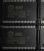
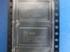
BS616UV2019TCG10: DescriptionThe BS616UV2019TCG10 is designed as a high performance, ultra low power CMOS static random access memory organized as 131,072 words by 16 bits and operated from a wide range of 1.8V to 3....
SeekIC Buyer Protection PLUS - newly updated for 2013!
268 Transactions
All payment methods are secure and covered by SeekIC Buyer Protection PLUS.
Features: • Very low operation voltage : 2.4 ~ 5.5V• Very low power consumption : Vcc ...
The BS616UV2019TCG10 is designed as a high performance, ultra low power CMOS static random access memory organized as 131,072 words by 16 bits and operated from a wide range of 1.8V to 3.6V supply voltage. Advanced CMOS technology and circuit techniques provide both high speed and low power features of BS616UV2019TCG10 with a typical CMOS standby current of 0.2uA at 2.0V, 25°C and maximum access time of 85ns at 85°C.
BS616UV2019TCG10 has six features. (1)Wide Vcc operation voltage. (2)Ultra low power consumption. (3)High speed access time which would be max 100ns. (4)Automativ power down when chip is deselected. (5)Three state outputs and TTL compatible. (6)Fully static operation. Those are all the main features.
Some absolute maximum ratings of BS616UV2019TCG10 have been concluded into several points as follow. (1)Its terminal voltage with respect to GND would be from -0.5V to Vcc+0.5V. (2)Its temperature under bias would be from -40°C to 85°C. (3)Its storage temperature range would be from -60°C to 150°C. (4)Its power dissipation would be 1.0W. (5)Its DC output current would be 20mA. It should be noted that stresses above those listed in absolute maximum ratings may cause permanent damage to device.
Also some electrical characteristics of BS616UV2019TCG10 are concluded as follow. (1)Its guaranteed input low voltage would be min -0.3V and max 0.8V. (2)Its guaranteed input high voltage would be min 1.4V and max Vcc+0.3V. (3)Its input leakage current would be max 1uA. (4)Its output leakage current would be max 1uA. (5)Its output low voltage would be max 0.2V at Vcc=2.0V and would be max 0.4V at Vcc=3.0V. (6)Its output high voltage would be min Vcc-0.2V at Vcc=2.0V and would be min 2.4V at Vcc=3.0V. (7)Its operating power supply current would be max 10mA at Vcc=2.0V and would be max 13mA at Vcc=3.0V. And so on. If you have any question or suggestion or want to know more information please contact us for details. Thank you!