SeekIC No. : 004303051
Detail
BTS 716G: Application• µC compatible high-side power switch with diagnostic feedback for 12V and 24V grounded loads• All types of resistive, inductive and capacitve loads• Most suitabl...
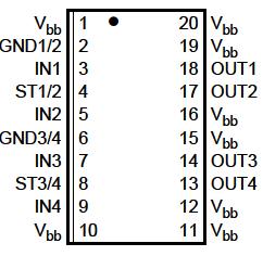
 BTS 716G Data Sheet
floor Price/Ceiling Price
- Part Number:
- BTS 716G
- Supply Ability:
- 5000
Price Break
- Qty
- 1~5000
- Unit Price
- Negotiable
- Processing time
- 15 Days
SeekIC Buyer Protection PLUS - newly updated for 2013!
- Escrow Protection.
- Guaranteed refunds.
- Secure payments.
- Learn more >>
Month Sales
268 Transactions
Payment Methods
All payment methods are secure and covered by SeekIC Buyer Protection PLUS.
Notice: When you place an order, your payment is made to SeekIC and not to your seller. SeekIC only pays the seller after confirming you have received your order. We will also never share your payment details with your seller.