Features: • High-Voltage Type (20V Rating)
• Set-Reset Capability
• Static Flip-Flop Operation - Retains State Indefinitely With Clock Level Either "High" Or "Low"
• Medium-Speed Operation - 16 MHz (typ.) Clock Toggle Rate at 10V
• Standardized Symmetrical Output Characteristics
• 100% Tested for Quiescent Current at 20V
• Maximum Input Current of 1A at 18V Over Full Package Temperature Range; 100nA at 18V and +25oC
• Noise Margin (Over Full Package Temperature Range):
1V at VDD = 5V
2V at VDD = 10V
2.5V at VDD = 15V
• 5V, 10V and 15V Parametric Ratings
• Meets All Requirements of JEDEC Tentative Standard No. 13B, "Standard Specifications for Description of 'B' Series CMOS Devices"
Application• Registers
• Counters
• Control Circuits
Pinout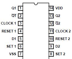 Specifications
DC Supply Voltage Range, (VDD) ... -0.5V to +20V (Voltage Referenced to VSS Terminals)
Input Voltage Range, All Inputs ...........................................................-0.5V to VDD +0.5V
DC Input Current, Any One Input.............................................................................±10mA
Operating Temperature Range ...................... -55 to +125Package Types D, F, K, H
Storage Temperature Range (TSTG) .................................................... . -65 to +150
Lead Temperature (During Soldering) .................................................................. +265
At Distance 1/16 ± 1/32 Inch (1.59mm ± 0.79mm) from case for 10s Maximum
DescriptionCD4013BMS consists of two identical, independent data type flip-flops. Each flip-flop has independent data, set, reset, and clock inputs and Q and Q outputs. These devices can be used for shift register applications, and, by connecting Q output to the data input, for counter and toggle applications. The logic level present at the D input is transferred to the Q output during the positive going transition of the clock pulse. Setting or resetting is independent of the clock and is accomplished by a high level on the set or reset line, respectively.
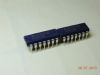
The CD4013BMS is supplied in these 14 lead outline packages:
Braze Seal DIP H4Q
Frit Seal DIP H1B
Ceramic Flatpack H3W

 CD4013BMS Data Sheet