Features: * High Voltage Types (20V Rating)
* Medium Speed Operation 12MHz (Typ.) Clock Rate at
VDD-VSS = 10V
* Fully Static Operation
* 8 Master-Slave Flip-Flops Plus Output Buffering and
Control Gating
* 100% Tested for Quiescent Current at 20V
* Maximum Input Current of 1A at 18V oOver Full Pack-
age Temperature Range; 100nA at 18V and +25
* Noise Margin (Full Package Temperature Range)
* 1V at VDD = 5V
* 2V at VDD = 10V
* 2.5V at VDD = 15V
* Standardized Symmetrical Output Characteristics
* 5V, 10V and 15V Parametric Ratings
* Meets All Requirements of JEDEC Tentative Standard
No. 13B, "Standard Specifications for Description of
`B' Series CMOS DevicesApplication* Parallel Input/Serial Output Data Queueing
* Parallel to Serial Data Conversion
* General Purpose RegisterPinout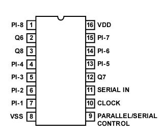 Specifications
DC Supply Voltage Range, (VDD) . . . . . . . . . . . . . . . -0.5V to +20V
(Voltage Referenced to VSS Terminals)
Input Voltage Range, All Inputs . . . . . . . . . . . . .-0.5V to VDD +0.5V
DC Input Current, Any One Input . . . . . . . . . .±10mA to +125
Operating Temperature Range. . . . . . . . . . . . . . . . . . . . . . . -55
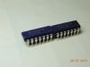
Package Types D, F, K, H
Storage Temperature Range (TSTG). . . . . . . . . . -65 to +150
Lead Temperature (During Soldering) . . . . . . . . . . . . . . . . . +265
At Distance 1/16 ± 1/32 Inch (1.59mm ± 0.79mm) from case for
10s Maximum
Description
CD4014BMS -Synchronous Parallel or Serial Input/Serial Output
CD4021BMS -Asynchronous Parallel Input or Synchronous Serial Input/Serial Output
Serial Input/Serial Output CD4014BMS and CD4021BMS series types are 8-stage paral- lel- or serial-input/serial output registers having common CLOCK and PARALLEL/SERIAL CONTROL inputs, a single SERIAL data input, and individual parallel "JAM" inputs to each register stage. Each register stage is a D-type, master-slave flip-flop. In addition to an output from stage 8, "Q" outputs are also available from stages 6 and 7. Parallel as well as serial entry is made into the register synchronously with the positive clock line transition in the CD4014BMS. In the CD4021BMS serial entry is synchronous with the clock but parallel entry is asynchronous. In both types, entry is controlled by the PARALLEL/SERIAL CONTROL input. When the PARALLEL/SERIAL CONTROL input is low, data is seri ally shifted into the 8-stage register synchronously with the positive transition of the clock line. When the PARAL LEL/ SERIAL CONTROL input is high, data is jammed into the 8- stage register via the parallel input lines and synch ronous with the positive transition of the clock line. In the CD4021BMS, the CLOCK input of the internal stage is "forced" when asynchronous parallel entry is made. Register expansion using multiple packages is permitted.
The CD4014BMS and CD4021BMS are supplied in these 16 lead outline packages:
Braze Seal DIP H4T
Frit Seal DIP H1F
Ceramic Flatpack H6W

 CD4014BMS Data Sheet