CD4015BMS

Features: • High-Voltage Type (20V Rating)• Medium Speed Operation 12MHz (typ.) Clock Rate at VDD - VSS = 10V• Fully Static Operation• 8 Master-Slave Flip-Flops Plus Input and Output Buffering• 100% Tested For Quiescent Current at 20V• 5V, 10V and 15V Parametric...

product image

CD4015BMS Picture
SeekIC No. : 004311192 Detail

CD4015BMS: Features: • High-Voltage Type (20V Rating)• Medium Speed Operation 12MHz (typ.) Clock Rate at VDD - VSS = 10V• Fully Static Operation• 8 Master-Slave Flip-Flops Plus Input an...

floor Price/Ceiling Price

Part Number:
CD4015BMS
Supply Ability:
5000

Price Break

  • Qty
  • 1~5000
  • Unit Price
  • Negotiable
  • Processing time
  • 15 Days
Total Cost: $ 0.00

SeekIC Buyer Protection PLUS - newly updated for 2013!

  • Escrow Protection.
  • Guaranteed refunds.
  • Secure payments.
  • Learn more >>

Month Sales

268 Transactions

Rating

evaluate  (4.8 stars)

Upload time: 2024/4/29

Payment Methods

All payment methods are secure and covered by SeekIC Buyer Protection PLUS.

Notice: When you place an order, your payment is made to SeekIC and not to your seller. SeekIC only pays the seller after confirming you have received your order. We will also never share your payment details with your seller.
Product Details

Description


Features:

• High-Voltage Type (20V Rating)
• Medium Speed Operation 12MHz (typ.) Clock Rate at VDD - VSS = 10V
• Fully Static Operation
• 8 Master-Slave Flip-Flops Plus Input and Output Buffering
• 100% Tested For Quiescent Current at 20V
• 5V, 10V and 15V Parametric Ratings
• Standardized Symmetrical Output Characteristics
• Maximum Input Current of 1A at 18V Over Full Package-Temperature Range; 100nA at 18V and 25
• Noise Margin (Full Package-Temperature Range) =
- 1V at VDD = 5V
- 2V at VDD = 10V
- 2.5V at VDD = 15V
• Meets All Requirements of JEDEC Tentative Standard No. 13B, "Standard Specifications for Description of 'B' Series CMOS Devices"


Application

• Serial-Input/Parallel-Output Data Queueing
• Serial to Parallel Data Conversion
• General-Purpose Register


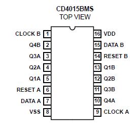
Pinout

  Connection Diagram


Specifications

DC Supply Voltage Range, (VDD) . . . . . . . . . . . . . . . -0.5V to +20V
(Voltage Referenced to VSS Terminals)
Input Voltage Range, All Inputs . . . . . . . . . .. . .-0.5V to VDD +0.5V
DC Input Current, Any One Input . . . . . . .. . .. . . . . . . . . . .±10mA
Operating Temperature Range. . . . . . . . . . . . . . . -55oC to +125
Package Types D, F, K, H
Storage Temperature Range (TSTG) . . . . . . . . . . . -65oC to +150
Lead Temperature (During Soldering) . . . . . . . . . . . . . . . . . +265


Description

CD4015BMS consists of two identical, independent, 4-stage serial-input/parallel output registers. Each register has independent CLOCK and RESET inputs as well as a single serial DATA input. Q outputs are available from each of the four stages on both registers. All register stages are D type, master- slave flip-flops. The logic level present at the DATA input is transferred into the first register stage and shifted over one stage at each positive-going clock transition. Resetting of all stages is accomplished by a high level on the reset line. Register expansion to 8 stages using one CD4015BMS package, or to more than 8 stages using additional CD4015BMSs is possible. The CD4015BMS is supplied in these 16 lead outline packages: Braze Seal DIP H4X Frit Seal DIP H1F Ceramic Flatpack H6W


Customers Who Bought This Item Also Bought

Margin,quality,low-cost products with low minimum orders. Secure your online payments with SeekIC Buyer Protection.
Audio Products
Fans, Thermal Management
Motors, Solenoids, Driver Boards/Modules
Circuit Protection
Batteries, Chargers, Holders
Discrete Semiconductor Products
View more