CD4027B

Features: SpecificationsDescriptionCD4027B is a single monolithic chip intergrated circuit containing two identical complementary-symmetry J-K master-slave flip-flops. It is useful in performing control, register and toggle functions. The typical applications include registers, counters and contro...

product image

CD4027B Picture
SeekIC No. : 004311245 Detail

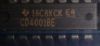
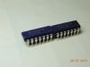
CD4027B: Features: SpecificationsDescriptionCD4027B is a single monolithic chip intergrated circuit containing two identical complementary-symmetry J-K master-slave flip-flops. It is useful in performing con...

floor Price/Ceiling Price

Part Number:
CD4027B
Supply Ability:
5000

Price Break

  • Qty
  • 1~5000
  • Unit Price
  • Negotiable
  • Processing time
  • 15 Days
Total Cost: $ 0.00

SeekIC Buyer Protection PLUS - newly updated for 2013!

  • Escrow Protection.
  • Guaranteed refunds.
  • Secure payments.
  • Learn more >>

Month Sales

268 Transactions

Rating

evaluate  (4.8 stars)

Upload time: 2024/4/29

Payment Methods

All payment methods are secure and covered by SeekIC Buyer Protection PLUS.

Notice: When you place an order, your payment is made to SeekIC and not to your seller. SeekIC only pays the seller after confirming you have received your order. We will also never share your payment details with your seller.
Product Details

Description


Features:


Specifications


Description

CD4027B is a single monolithic chip intergrated circuit containing two identical complementary-symmetry J-K master-slave flip-flops. It is useful in performing control, register and toggle functions. The typical applications include registers, counters and control circuits.

There are some CD4027B features as follows. First is set-reset capability. The second is static flip-flop operation which retains state indefinitely with clock level either "high" or "low". Then is medium speed operation which is 16 MHz (typ.) clock toggle rates at 10 V. Next is standardized symmetrical output characteristics. The fifth is 100% tested for quiescent current at 20 V. The sixth is maximum input current of 1A at 18 V over full package temperature range and 100 nA at 18 V and 25. The seventh is 5 V, 10 V and 15 V parametric ratings.

What comes next is about the CD4027B absolute maximum ratings. The VDD (DC supply voltage range (voltages referenced to VSS terminal)) is from -0.5 to +20 V. The input voltage range for all inputs is from -0.5 to VDD+0.5 V. The CD4027B DC input current for any one input is ±10 mA. The PD (power dissipation per package) is 500 mW for TA=-55 to +100 and derates linearity at 12 mW/ to 200 mW for TA=+100 to +125. The device dissipation per output transistor is 100 mW for TA=full package-temperature range (all package types). The Tstg (storage temperature range) is from -65 to +150. The TA (operating temperature range) is from -55 to +125. The CD4027B lad temperature (during soldering) is +265 at distance 1/16±1/32 inch (1.59±0.79mm) from case for 10 s max.


Customers Who Bought This Item Also Bought

Margin,quality,low-cost products with low minimum orders. Secure your online payments with SeekIC Buyer Protection.
Resistors
Fans, Thermal Management
Circuit Protection
Programmers, Development Systems
View more