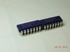
DescriptionCD4027B is a single monolithic chip integrated circuit containing two identical complementary-symmetry J-K master slave flip-flops.Each flip-flop has provisions for individual J, K,set, reset, and clock input signals. buffered Q and Q signals are provided as outputs. CD4027BF input- output arrangement provides for compatible operation with the RCA-CD4013B dual Da type flip-flop. The CD4027B is useful in performing control, register, and toggle functions. Logic levels present at the and inputs along with internal self-steering control the state of each flip-flop; changes in the flip-flop state are synchronous with the positive- going transition of the clock pulse. Set and reset functions are independent of the clock and are initiated when a high level signal is present at either the Set or Reset input. The CD4027B types are supplied in 16-lead hermetic dual-in-line ceramic packages (F3A suffix), 16-lead dual-in-line plastic packages (E suffix), 16-lead small-outline packages M96, M11 and NSR suffixes), and 16-lead thin shrink small-outline packages (PW and PWR suffixes).
The features of CD4027BF can be summarized as (1)set-reset capability; (2)static flip-flop operation - retains state indefinitely with clock level either "high" or "low"; (3)medium speed operation - 16 MHz(tye.) clock toggle rate at 10 V; (4)standardized symmetrical output characterietics; (5)100% tested for quieseent current at 20 V; (6)maximum input current of 1A pit at 18V over full package-temperature range; 100 nA at 18 V and 25°C; (7)noise margin (over full package- temperature range): 1 V at VDD = 5 V, 2 at VDD = 10 V, 2.5V at VDD =15 V.; (8)5-V, 10-V, and 15-V parametric ratings; (9)meets all requirements-of JEDEC Tentative Standard No. 13B, "standard specifications for description of 'B' series CMOS devices".
The absolute maximum ratings of CD4027BFare (1)DC supply-voltage range,(VDD) voltages referenced to VSS terminal): -0.5V to +20V; (2)input voltage range, all inputs: -0.5V to VDD+0.5V; (3)DC input current, any one input: ±10mA; (4)power dissipation per package: for TA=-55°C to +100°C:500mW; (5)for TA=+100°C to+125°C: degate linearity at 12mW/°C to 200mW/°C; (6)dvice dissipation per output transistor for TA= full package-temperature range (all package types): 100mW; (7)operating-temperature range: -55°C to +125°C; (8)storage temperature range (Tstg): -65°C to +150°C; (9)temperature (during soldering): at distance 1/16 ±1/32 inch (1.59±0.79mm) from case for 10s max +265°C.

 CD4027BF Data Sheet