Features: Wide supply voltage range 3.0V to 15V
High noise immunity 0.45 VDD (typ.)
Low power TTL fan out of 2 driving 74L compatibility or 1 driving 74LS
Fully static operation DC to 8 MHz VDD e 10V (typ.)
Fully buffered clock input 5 pF (typ.) input capacitance
Single phase clocking requirements
Delayed clock output for reduced clock drive requirements
Fully buffered outputs
High current sinking capability 1.6 mA
Q output @ VDD= 5V and 25
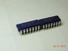
Pinout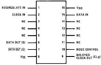 Specifications
Supply Voltage (VDD) ......................................................-0.5V to a18V
Input Voltage (VIN) ................................................-0.5V to VDD a0.5V
Storage Temperature Range (TS) ..............................-65 to a150
Power Dissipation (PD)
Dual-In-Line ............................................................................700 mW
Small Outline ..........................................................................500 mW
Lead Temp. (TL) (Soldering, 10 sec.).......................................... 260
DescriptionThe CD4031BM/CD4031BC is an integrated, complementary MOS (CMOS), 64-stage, fully static shift register. Two data inputs, DATA IN and RECIRCULATE IN, and a MODE CONTROL input are provided. Data at the DATA input (when MODE CONTROL is low) or data at the RECIRCULATE input (when MODE CONTROL is high), which meets the setup and hold time requirements, is entered into the first stage of the register and is shifted one stage at each positive transition of the CLOCK.
CD4031BM Data output is available in both true and complement forms from the 64th stage. Both the DATA OUT (Q) AND DATA OUT (Q )outputs are fully buffered.
The CLOCK input of the CD4031BM/CD4031BC is fully buffered, and present only a standard input load capacitance. However, a DELAYED CLOCK OUTPUT (CLD) has been provided to allow reduced clock drive fan-out and transition time requirements when cascading packages.

 CD4031BM Data Sheet