CD4041UBMS

Features: • High Voltage Type (20V Rating)• Balanced Sink and Source Current; Approximately 4 Times Standard B Drive• Equalized Delay to True and Complement Outputs• 100% Tested for Quiescent Current at 20V• Maximum Input Current of 1A at 18V Over Full Package-Tempe...

product image

CD4041UBMS Picture
SeekIC No. : 004311273 Detail

CD4041UBMS: Features: • High Voltage Type (20V Rating)• Balanced Sink and Source Current; Approximately 4 Times Standard B Drive• Equalized Delay to True and Complement Outputs• 100% T...

floor Price/Ceiling Price

Part Number:
CD4041UBMS
Supply Ability:
5000

Price Break

  • Qty
  • 1~5000
  • Unit Price
  • Negotiable
  • Processing time
  • 15 Days
Total Cost: $ 0.00

SeekIC Buyer Protection PLUS - newly updated for 2013!

  • Escrow Protection.
  • Guaranteed refunds.
  • Secure payments.
  • Learn more >>

Month Sales

268 Transactions

Rating

evaluate  (4.8 stars)

Upload time: 2024/5/9

Payment Methods

All payment methods are secure and covered by SeekIC Buyer Protection PLUS.

Notice: When you place an order, your payment is made to SeekIC and not to your seller. SeekIC only pays the seller after confirming you have received your order. We will also never share your payment details with your seller.
Product Details

Description


Features:

• High Voltage Type (20V Rating)
• Balanced Sink and Source Current; Approximately 4 Times Standard "B" Drive
• Equalized Delay to True and Complement Outputs
• 100% Tested for Quiescent Current at 20V
• Maximum Input Current of 1A at 18V Over Full
   Package-Temperature Range;
   - 100nA at 18V and +25oC
• 5V, 10V and 15V Parametric Ratings
• Meets All Requirements of JEDEC Tentative Standard No. 13B, "Standard Specificationsfor Description of 'B' Series CMOS Devices"


Application

• High Current Source/Sink Driver
• CMOS-to-DTL/TTL Converter Buffer
• Display Driver
• MOS Clock Driver
• Resistor Network Driver (Ladder or Weighted R)
• Buffer
• Transmission Line Driver


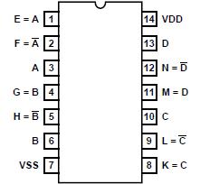
Pinout

  Connection Diagram


Specifications

DC Supply Voltage Range, (VDD) . . . . . . . . . . . . . . . .-0.5V to +20V
     (Voltage Referenced to VSS Terminals)
Input Voltage Range, All Inputs . . . . . . . . . . . . . -0.5V to VDD +0.5V
DC Input Current, Any One Input. . . . . . . . . . . . . . . . . . . . . . . . .±10mA
Operating Temperature Range . . . . . . . . . . . . . . . -55 to +125
    Package Types D, F, K, H
Storage Temperature Range (TSTG). . . . . . . . . . . -65to +150
Lead Temperature (During Soldering) . . . . . . . . . . . . . . . . . +265
     At Distance 1/16 ± 1/32 Inch (1.59mm ± 0.79mm) from case for 10s Maximum


Description

CD4041UBMS types are quad true/complement buffers consisting of n- and p- channel units having low channel resistance and high current (sourcing and sinking) capability. The CD4041UBMS is intended for use as a buffer, line driver, or CMOS-to-TTL driver. It can be used as an ultra-low power resistor-network driver for A/D and D/A conversion, as a transmission-line driver, and in other applications where high noise immunity and low power dissipation are primary design requirements.
The CD4041UBMS is supplied in these 14 lead outline packages:
       Braze Seal DIP                 H4Q
       Frit Seal DIP                     H1B
       Ceramic Flatpack             H3W


Customers Who Bought This Item Also Bought

Margin,quality,low-cost products with low minimum orders. Secure your online payments with SeekIC Buyer Protection.
Cables, Wires - Management
Semiconductor Modules
Crystals and Oscillators
Power Supplies - External/Internal (Off-Board)
Static Control, ESD, Clean Room Products
View more