CD4046BMS

Features: Very Low Power Consumption: 70W (typ.) at VCO fo = 10kHz, VDD = 5VOperating Frequency Range Up to 1.4 MHz (typ.) at VDD = 10V, RI = 5kLow Frequency Drift: 0.04%/ C (typ.) at VDD = 10VChoice of Two Phase Comparators: - Exclusive-OR Network (I)- Edge-Controlled Memory Network with Phase-Pu...

product image

CD4046BMS Picture
SeekIC No. : 004311289 Detail

CD4046BMS: Features: Very Low Power Consumption: 70W (typ.) at VCO fo = 10kHz, VDD = 5VOperating Frequency Range Up to 1.4 MHz (typ.) at VDD = 10V, RI = 5kLow Frequency Drift: 0.04%/ C (typ.) at VDD = 10VChoic...

floor Price/Ceiling Price

Part Number:
CD4046BMS
Supply Ability:
5000

Price Break

  • Qty
  • 1~5000
  • Unit Price
  • Negotiable
  • Processing time
  • 15 Days
Total Cost: $ 0.00

SeekIC Buyer Protection PLUS - newly updated for 2013!

  • Escrow Protection.
  • Guaranteed refunds.
  • Secure payments.
  • Learn more >>

Month Sales

268 Transactions

Rating

evaluate  (4.8 stars)

Upload time: 2024/4/23

Payment Methods

All payment methods are secure and covered by SeekIC Buyer Protection PLUS.

Notice: When you place an order, your payment is made to SeekIC and not to your seller. SeekIC only pays the seller after confirming you have received your order. We will also never share your payment details with your seller.
Product Details

Description


Features:

Very Low Power Consumption:
    70W (typ.) at VCO fo = 10kHz, VDD = 5V
Operating Frequency Range Up to 1.4 MHz (typ.) at
    VDD = 10V, RI = 5k
Low Frequency Drift: 0.04%/ C (typ.) at VDD = 10V
Choice of Two Phase Comparators:
   - Exclusive-OR Network (I)
   - Edge-Controlled Memory Network with Phase-Pulse
  Output for Lock Indication (II)
High VCO Linearity: <1% (typ.) at VDD = 10V
VCO Inhibit Control for ON-OFF Keying and Ultra-Low
    Standby Power Consumption
Source-Follower Output of VCO Control Input
   (Demod. Output)
Zener Diode to Assist Supply Regulation
Standardize, Symmetrical Output Characteristics
100% Tested for Quiescent Current at 20V
5V, 10V and 15V Parametric Ratings
Meets All Requirements of JEDEC Tentative Standard
   No. 13B, "Standard Specifications for Description of 'B'
   Series CMOS Devices"


Application

 FM Demodulator and Modulator
Frequency Synthesis and Multiplication
Frequency Discriminator
Data Synchronization
Voltage-to-Frequency Conversion
Tone Decoding
FSK - Modems
Signal Conditioning


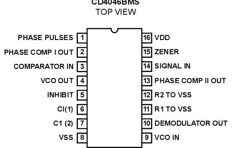
Pinout

  Connection Diagram


Specifications

DC Supply Voltage Range, (VDD) . . . . . . . . . . . . . ......... . -0.5V to +20V
(Voltage Referenced to VSS Terminals)
Input Voltage Range, All Inputs . . . . . . . . . . ....... . .-0.5V to VDD +0.5V
DC Input Current, Any One Input . . . . . . . . . . . . . . . . . . . . . . . .±10mA
Operating Temperature Range. . . . . . . . . . . . ........ . . . -55 C to +125
Package Types D, F, K, H
Storage Temperature Range (TSTG). . . . . . . . . .......... . -65 C to +150

Lead Temperature (During Soldering) . . . . . . . . . . . . . . ....... . . +265


Description

CD4046BMS CMOS Micropower Phase-Locked Loop (PLL) consists of a low power linear voltage-controlled oscillator (VCO) and two different phase comparators having a common signal- input amplifier and a common comparator input. A 5.2V zener diode is provided for supply regulation if necessary.

The CD4046BMS is supplied in these 16-lead outline packages:


Customers Who Bought This Item Also Bought

Margin,quality,low-cost products with low minimum orders. Secure your online payments with SeekIC Buyer Protection.
Transformers
Optoelectronics
Resistors
Semiconductor Modules
Boxes, Enclosures, Racks
Prototyping Products
DE1
View more