Supply Current
:
Supply Voltage - Min
: 3 V
On Resistance (Max)
: 1050 Ohms
Supply Voltage - Max
: 20 V
Maximum Operating Temperature
: + 125 C
Minimum Operating Temperature
: - 55 C
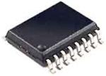
Package / Case
: SOIC-16
Number of Channels
: 3 Channel
Packaging
: Tube
Propagation Delay Time
: 60 ns
On Time (Max)
: 720 ns
Off Time (Max)
: 450 ns
Maximum Power Dissipation
: 700 mW
Features: Wide range of digital and analog signal levels: digital 3±15V, analog to 15Vp-p
Low ``ON'' resistance: 80X (typ.) over entire 15Vp-p signal- input range for VDD-VEEe15V
High ``OFF'' resistance: channel leakage of g10 pA (typ.) at VDD-VEEe10V
Logic level conversion for digital addressing signals of 3±15V (VDD-VSSe3±15V) to switch analog signals to 15 Vp-p (VDD-VEEe15V)
Matched switch characteristics: DRONe5X (typ.) for VDD-VEEe15V
Very low quiescent power dissipation under all digitalcontrol input and supply conditions: 1 mW (typ.) at VDD-VSSeVDD-VEEe10V
Binary address decoding on chip
SpecificationsIf Military/Aerospace specified devices are required, please contact the National Semiconductor Sales Office/Distributors for availability and specifications.
DC Supply Voltage (VDD) -0.5 VDC to a18 VDC
Input Voltage (VIN) -0.5 VDC to VDDa0.5 VDC
Storage Temperature Range (TS) -65.C to a150.C
Power Dissipation (PD)
Dual-In-Line 700 mW
Small Outline 500 mW
Lead Temp. (TL) (soldering, 10 sec.) 260.C
Recommended Operating Conditions
DC Supply Voltage (VDD) +5 VDC to +15 VDC
Input Voltage (VIN) 0V to VDD VDC
Operating Temperature Range (TA)
4051BM/4052BM/4053BM -55.C to +125.C
4051BC/4052BC/4053BC -40.C to +85.C
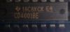
DescriptionThese CD4053BM analog multiplexers/demultiplexers are digitally controlled analog switches having low ``ON'' impedance and very low ``OFF'' leakage currents. Control of analog signals up to 15Vp-p can be achieved by digital signal mplitudes of 3±15V. For example, if VDDe5V, VSSe0V and VEEeb5V, CD4053BM analog signals from b5V to a5V can be controlled by digital inputs of 0±5V. The multiplexer circuits dissipate extremely low quiescent power over the full VDD-VSS and VDD-VEE supply voltage ranges, independent of the logic state of the control signals. When a logical ``1'' is present at the inhibit input terminal all channels are ``OFF''.
CD4051BM/CD4051BC is a single 8-channel multiplexer having three binary control inputs. A, B, and C, and an inhibit input. The three binary signals select 1 of 8 channels to be turned ``ON'' and connect the input to the output.
CD4052BM/CD4052BC is a differential 4-channel multiplexer having two binary control inputs, A and B, and an inhibit input. The two binary input signals select 1 or 4 pairs of channels to be turned on and connect the differential analog
inputs to the differential outputs.
CD4053BM/CD4053BC is a triple 2-channel multiplexer having three separate digital control inputs, A, B, and C, and an inhibit input. Each control input selects one of a pair of channels which are connected in a single-pole double-throw configuration.
Parameters: | Technical/Catalog Information | CD4053BM |
| Vendor | Texas Instruments |
| Category | Integrated Circuits (ICs) |
| Type | Multiplexer/Demultiplexer |
| Voltage Supply Source | Dual Supply |
| Voltage - Supply, Single/Dual (±) | ±3 V ~ 20 V |
| Circuit | 3 x 2:1 |
| On-State Resistance | 240 Ohm |
| Mounting Type | Surface Mount |
| Package / Case | 16-SOIC (3.9mm Width) |
| Packaging | Tube |
| Current - Supply | .08A |
| Operating Temperature | -55°C ~ 125°C |
| Function | Multiplexer/Demultiplexer |
| Drawing Number | 296; 4040047-4; D; 16 |
| Lead Free Status | Lead Free |
| RoHS Status | RoHS Compliant |
| Other Names | CD4053BM
CD4053BM
|
 CD4053BM Data Sheet