Maximum Operating Temperature
: + 125 C
Number of Gates
: 1
Packaging
: Tube
Mounting Style
: Through Hole
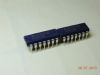
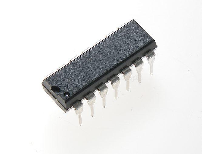
Package / Case
: PDIP-14
High Level Output Current
: - 4.2 mA
Low Level Output Current
: 4.2 mA
Supply Voltage - Max
: 18 V
Supply Voltage - Min
: 3 V
Product
: MUX Gates
Propagation Delay Time
: 620 ns
Logic Family
: CD40
Number of Lines (Input / Output)
: 4 Wide 2-IN / 1
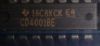
DescriptionThe CD4086BE belongs to CD4Q86B family which contains one 4-wide 2-inputAND-OR-INVERT gate with an lNHlBlT/EXP A input, endmg an ENABLE/EXP input. For a 4-wide A-O-function INHIBITIT is tied to and ENABLE/EXP to Vbg. See Fig.10 and its associated explanation for applications where a capability greater than 4-wide is required. The CD4086B types are supplied in 14-leadhermetic dual-in-line ceramic packages (F3A suffix), 14-lead dual-in-line plastic packages (E suffix), 14-lead small-outline packages MT, M96, and NSR suffixes), and 14-lead thin shrink small-outline packages (PW and PWR suffixes).
The features of CD4086BE can be summarized as (1)medium-speed operation-tpHL 90 ns; tpLH-140ns(typ.) at 10 V; (2)INHIBIT and ENABLE inputs; (3)buffered outputs; (4)100%teated for quiescent current at 20 V; (5)CD4086BE maximum input leakage currant of 18 Vover full package-temperature rang; 100 nA at 18 V and 25°C; (6)noise margin (over full package temperature range): 1V at VDD=5V, 2V at VDD=10 V, 2.5 at VDD 15V; (7)standardized, symmetrical output characteristics; (8)5-V, 10-V, and 15-V parametric ratings; (9)meets all requirements of JEDEC tentative standard No. 13B, "standard specifications for description of series CMQS devices".
The absolute maximum ratings of CD4086BE are (1)DC supply-voltage range, (VDD) voltages referenced to VSS terminal): -0.5V to +20V; (2)input voltage range, all inputs: -0.5V to VDD +0.5V; (3)DC input current anyone input: ±10mA; (4)power dissipation per package (PD): for TA -55°C to +100°C: 500mW, for TA = +100°C to 125°C: derate linearly at 12mW/°C to 200mW; (5)CD4086BE device dissipation per output transistor for TA=full package-temperature range (all package types): 100mW; (6)operating-temperature range (TA):-55°C to +125°C; (7)storage temperature range (Tstg): -65°C +150°C; (8)lead temperature (during solderingi): at dlelance 1/16 ± 1/32 inch(1.59±0.79mm) from case for 10s max: +265°C.
Parameters: | Technical/Catalog Information | CD4086BE |
| Vendor | Texas Instruments |
| Category | Integrated Circuits (ICs) |
| Number of Circuits | 1 - Single |
| Logic Type | 2 Input AND-OR-INVERT |
| Current - Output High, Low | 6.8mA, 6.8mA |
| Output Type | Single-Ended |
| Schmitt Trigger Input | No |
| Voltage - Supply | 3 V ~ 18 V |
| Operating Temperature | -55°C ~ 125°C |
| Number of Inputs | 2 |
| Mounting Type | Through Hole |
| Package / Case | 14-DIP (300 mil) |
| Packaging | Tube |
| Drawing Number | 296; 4040049; N; 14, 16, 18, 20 |
| Lead Free Status | Lead Free |
| RoHS Status | RoHS Compliant |
| Other Names | CD4086BE
CD4086BE
296 14281 5 ND
296142815ND
296-14281-5
|
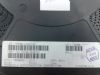
 CD4086BE Data Sheet