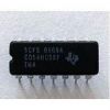
CD54ACT2993A

SpecificationsDC Supply Voltage, VCC. . . . . . . . . . . . . . . . . . . . . . . . . . . .. . . . . . . . -0.5V to +6VDC Input Diode Current, IIKFor VI < -0.5V or VI > VCC + 0.5V . . . . . . . . . . . . . . . . . . . . . . . . . . . . . . . .±20mADC Output Diode Current, IOKFor VO < -0.5...

product image

CD54ACT2993A Picture
SeekIC No. : 004311581 Detail

CD54ACT2993A: SpecificationsDC Supply Voltage, VCC. . . . . . . . . . . . . . . . . . . . . . . . . . . .. . . . . . . . -0.5V to +6VDC Input Diode Current, IIKFor VI < -0.5V or VI > VCC + 0.5V . . . . . . ...

floor Price/Ceiling Price

Part Number:
CD54ACT2993A
Supply Ability:
5000

Price Break

  • Qty
  • 1~5000
  • Unit Price
  • Negotiable
  • Processing time
  • 15 Days
Total Cost: $ 0.00

SeekIC Buyer Protection PLUS - newly updated for 2013!

  • Escrow Protection.
  • Guaranteed refunds.
  • Secure payments.
  • Learn more >>

Month Sales

268 Transactions

Rating

evaluate  (4.8 stars)

Upload time: 2024/4/29

Payment Methods

All payment methods are secure and covered by SeekIC Buyer Protection PLUS.

Notice: When you place an order, your payment is made to SeekIC and not to your seller. SeekIC only pays the seller after confirming you have received your order. We will also never share your payment details with your seller.
Product Details

Description


Specifications

DC Supply Voltage, VCC. . . . . . . . . . . . . . . .  . . . . . .  . . . . . .. . . . . . . . -0.5V to +6V
DC Input Diode Current, IIK
For VI < -0.5V or VI > VCC + 0.5V . . . . . . . . . . . .  . . . . . .  . . . . . . . . . . . . . .±20mA
DC Output Diode Current, IOK
For VO < -0.5V or VO > VCC + 0.5V. . . . . . . . . .  . . . . . .  . . . . .. . . . . . . . . . .±50mA
DC Output Source or Sink Current, Per Output Pin, IO
For VO > -0.5V or VO < VCC + 0.5V. . . . . . . . . . . . .  . . . . . .  . . . . ..  . . . . . . .±50mA
DC VCC or GND Current, ICC or IGND
For Up to 4 Outputs Per Device, Add ±25mA For Each
Additional Output . . . . . . . . . . . . . . . . . . . . . . . . . . .  . . .  . . . . . . . . . . . . . .±100mA
Power Dissipation Per Package, PD
TA = -55 to +100 (Package F) . . . . . . . . .  . . . . . .  . . . . . .  . . . . . . . . . . . 500mW
TA = +100 to +125 (Package F) . . . . . . . . . Derate Linearly at 8mW/ to 300mW
Operating Temperature Range, TA
Package Type F . . . . . . . . . . . . . . . . . . . .  . . . . . .  . . . . . .  . . . . .  . . -55 to +125
Storage Temperature, TSTG . . . . . . . . . . ... . . . . . .  . . . . . .  . . . .   . . -65 to +150
Lead Temperature (During Soldering)
At Distance 1/16in. ± 1/32in. (1.59mm ± 0.79mm)
From Case For 10s Max . . . . . . . . . . . . . . . . . . . . . . . . . . .  . . . . . .  . . . . . . .. . +265
Unit Inserted Into a PC Board (Min Thickness 1/16in., 1.59mm)
With Solder Contacting Lead Tips Only. . . . . . . .  . . . . . .  . . . . . .  . . . . . . . . . . +300


Description

The CD54AC299/3A and CD54ACT299/3A are three-state, 8-input universal shift/storage registers with common parallel I/O pins. CD54ACT2993A utilize the Harris Advanced CMOS Logic technology. These registers have four synchronous operating modes controlled by the two select inputs as shown in the Mode Select (S0, S1) table. CD54ACT2993A Select, the Serial Data (DS0, DS7), and the Parallel Data (I/O0 - I/O7) respond only to the LOW-to-HIGH transition of the clock pulse (CP). S0, S1 and Data inputs must be present one setup time prior to the positive transition of the clock.

The CD54ACT2993A Master Reset (MR) is an asynchronous active-LOW input. When MR is LOW, the register is cleared regardless of the status of all other inputs. The register can be expanded by cascading same units by tying the serial output (QO) to the serial data (DS7) input of the preceding register, and tying the serial output (Q7) to the serial data (DS0) input of the following register. Recirculating the (n x 8) bits is accomplished by tying the Q7 of the last stage to the DS0 of the first stage.
The three-state input/output (I/O) port has three modes of operation

1. CD54ACT2993A Both Output Enable (OE1 and OE2) inputs are LOW and S0 or S1 or both are LOW, the data in the register is present at the eight outputs.

2. When CD54ACT2993A both S0 and S1 are HIGH, I/O terminals are in the high-impedance state but being input ports, ready for parallel data to be loaded into eight registers with one clock transition regardless of the status of OE1 and OE2.

3. Either one of the two Output Enable inputs being HIGH will force I/O terminals to be in the off state. CD54ACT2993A is noted that each I/O terminal is a three-state output and a CMOS buffer input.

The CD54AC299/3A and CD54ACT299/3A are supplied in 20 lead dual-in-line ceramic packages (F suffix).


Customers Who Bought This Item Also Bought

Margin,quality,low-cost products with low minimum orders. Secure your online payments with SeekIC Buyer Protection.
Transformers
Prototyping Products
DE1
Circuit Protection
Power Supplies - Board Mount
RF and RFID
Motors, Solenoids, Driver Boards/Modules
View more