CD54HC373

Features: `2-V to 6-V VCC Operation`Wide Operating Temperature Range of 55 to 125`Balanced Propagation Delays and`Transition Times`Standard Outputs Drive up to 15 LS-TTL Loads`Significant Power Reduction Compared to LS-TTL Logic ICsPinoutSpecificationsSupply voltage range, VCC . . . . . . . . . . ...

product image

CD54HC373 Picture
SeekIC No. : 004311680 Detail

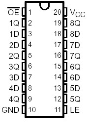
CD54HC373: Features: `2-V to 6-V VCC Operation`Wide Operating Temperature Range of 55 to 125`Balanced Propagation Delays and`Transition Times`Standard Outputs Drive up to 15 LS-TTL Loads`Significant Power Redu...

floor Price/Ceiling Price

Part Number:
CD54HC373
Supply Ability:
5000

Price Break

  • Qty
  • 1~5000
  • Unit Price
  • Negotiable
  • Processing time
  • 15 Days
Total Cost: $ 0.00

SeekIC Buyer Protection PLUS - newly updated for 2013!

  • Escrow Protection.
  • Guaranteed refunds.
  • Secure payments.
  • Learn more >>

Month Sales

268 Transactions

Rating

evaluate  (4.8 stars)

Upload time: 2024/4/29

Payment Methods

All payment methods are secure and covered by SeekIC Buyer Protection PLUS.

Notice: When you place an order, your payment is made to SeekIC and not to your seller. SeekIC only pays the seller after confirming you have received your order. We will also never share your payment details with your seller.
Product Details

Description


Features:

`2-V to 6-V VCC Operation
`Wide Operating Temperature Range of 55 to 125
`Balanced Propagation Delays and
`Transition Times
`Standard Outputs Drive up to 15 LS-TTL Loads
`Significant Power Reduction Compared to LS-TTL Logic ICs


Pinout

  Connection Diagram


Specifications

Supply voltage range, VCC  . . . . . . . . . . . . . . . . . . . . . . . . . . . . . . . . . . . .. . . . .. . . .0.5 V to 7 V
Input clamp current, IIK (VI < 0 or VI > VCC) (see Note 1) . . . . . . . . . . . . . . . . . . . . . . . . ±20 mA
Output clamp current, IOK (VO < 0 or VO > VCC) (see Note 1)  . . . . . . . . . . . . . . . . . . . . .±20 mA
Continuous output drain current per output, IO (VO = 0 to VCC) . . . . . . . . . . . . . . . . . . .  ±35 mA
Continuous output source or sink current per output, IO (VO = 0 to VCC)  . . . . . . . . . . . . ±25 mA
Continuous current through VCC or GND  . . . . . . . . . . . . . . . . . . . . . . . . . . . . . . . . . . . . . .±50 mA
Package thermal impedance, JA (see Note 2): E package. . . . . . . . . . . . . . . . . . .. . . . . . . 69/W
                                                                          M package  . . . . . . . . . . . . . . . . . . . . . . . . .58/W
Storage temperature range, Tstg  . . . . . . . . . . . . . . . . . . . . . . . . . . . . . . . . . . . . . .65 to 150


Description

The 'HC373 devices are octal transparent D-type latches designed for 2-V to 6-V VCC operation.

When theCD54HC373  latch-enable (LE) input is high, the Q outputs follow the data (D) inputs. When LE is low, the Q outputs are latched at the logic levels of the D inputs.

A buffered output-enable (OE) input can be used to place the eight outputs in either a normal logic state (high or low) or the high-impedance state. In the high-impedance state, the outputs neither load nor drive the bus lines significantly. The CD54HC373 high-impedance state and increased drive provide the capability to drive bus lines without interface or pullup components.

OE does not affect the internal operations of the latches. Old data can be retained or new data can be entered while the outputs are in the high-impedance state.

To ensure the high-impedance state during power up or power down, OE should be tied to VCC through a pullup resistor; the CD54HC373 minimum value of the resistor is determined by the current-sinking capability of the driver.


Customers Who Bought This Item Also Bought

Margin,quality,low-cost products with low minimum orders. Secure your online payments with SeekIC Buyer Protection.
Boxes, Enclosures, Racks
Optical Inspection Equipment
Undefined Category
Cables, Wires
Discrete Semiconductor Products
Sensors, Transducers
View more