Features: AC Types Feature 1.5-V to 5.5-V Operation and Balanced Noise Immunity at 30% of the Supply Voltage
Speed of Bipolar F, AS, and S, With Significantly Reduced Power Consumption
Balanced Propagation Delays
±24-mA Output Drive Current Fanout to 15 F Devices
SCR-Latchup-Resistant CMOS Process and Circuit Design
Exceeds 2-kV ESD Protection Per MIL-STD-883, Method 3015
ApplicationAudio
Automotive
Broadband
Digital Control
Military
Optical Networking
Security
Telephony
Video & Imaging
Wireless
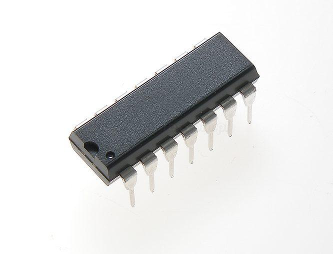
Pinout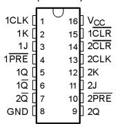 Specifications
Supply voltage range, VCC . . . . . . . . . . . . . . . . . . . . . . . . . . . . . . . . . . . . . . . . . . . . . . . . . . . . . . . . . . 0.5 V to 6 V
Input clamp current, I IK (V < 0 V or VI > VCC ) (see Note 1) . . . . . . . . . . ± 20 mA
Output clamp current, IOK (V O < 0 V or V O > VCC ) (see Note 1) . . . . . .± 50 mA
Continuous output current, IO (V O > 0 V or VO < V CC) . . . . . . . . . . . . . ± 50 mA
Continuous current through V CC or GND . . . . . . . . . . . . . . . . . . . . . . . . . ±00 mA
Package thermal impedance, JA (see Note 2): E package . . . . . . . . . . . .67°C/W
M package . . . . . . . . . . .73°C/W
Storage temperature range, TSTG . . . . . . . . . . . . . . . . . . . . . . . . .65 to 150
DescriptionThe 'AC112 devices contain two independent J-K negative-edge-triggered flip-flops. A low level at the preset (PRE) or clear (CLR) inputs sets or resets the outputs, regardless of the levels of the other inputs. When PRE and CLR are inactive (high), data at the J and K inputs meeting the setup-time requirements is transferred to the outputs on the negative-going edge of the clock pulse (CLK). Clock triggering occurs at a voltage level and is not directly related to the fall time of the clock pulse. Following the hold-time interval, data at the J and K inputs may be changed without affecting the levels at the outputs. These CD74AC112 versatile flip-flops can perform as toggle flip-flops by tying J and K high.

 CD74AC112 Data Sheet