CD74FCT2952A

Features: BiCMOS Technology With Low Quiescent PowerBuffered InputsNoninverted OutputsInput/Output Isolation From VCCControlled Output Edge Rates64-mA Output Sink CurrentOutput Voltage Swing Limited to 3.7 V at VCC = 5 VSCR Latch-Up-Resistant BiCMOS Process and Circuit DesignPackaged in Plastic Sm...

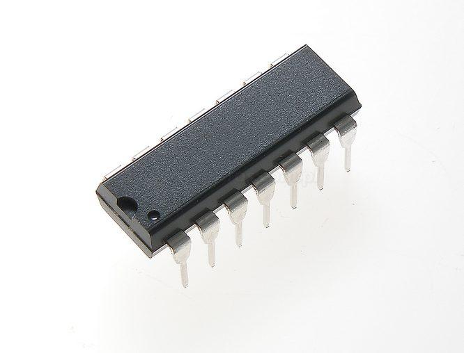
product image

CD74FCT2952A Picture
SeekIC No. : 004311927 Detail

CD74FCT2952A: Features: BiCMOS Technology With Low Quiescent PowerBuffered InputsNoninverted OutputsInput/Output Isolation From VCCControlled Output Edge Rates64-mA Output Sink CurrentOutput Voltage Swing Limited...

floor Price/Ceiling Price

Part Number:
CD74FCT2952A
Supply Ability:
5000

Price Break

  • Qty
  • 1~5000
  • Unit Price
  • Negotiable
  • Processing time
  • 15 Days
Total Cost: $ 0.00

SeekIC Buyer Protection PLUS - newly updated for 2013!

  • Escrow Protection.
  • Guaranteed refunds.
  • Secure payments.
  • Learn more >>

Month Sales

268 Transactions

Rating

evaluate  (4.8 stars)

Upload time: 2024/4/27

Payment Methods

All payment methods are secure and covered by SeekIC Buyer Protection PLUS.

Notice: When you place an order, your payment is made to SeekIC and not to your seller. SeekIC only pays the seller after confirming you have received your order. We will also never share your payment details with your seller.
Product Details

Description


Features:

 BiCMOS Technology With Low Quiescent Power
 Buffered Inputs
 Noninverted Outputs
 Input/Output Isolation From VCC
 Controlled Output Edge Rates
 64-mA Output Sink Current
 Output Voltage Swing Limited to 3.7 V at VCC = 5 V
 SCR Latch-Up-Resistant BiCMOS Process and Circuit Design
 Packaged in Plastic Small-Outline Package


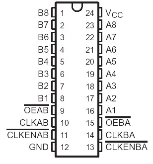
Pinout

  Connection Diagram


Specifications

DC supply voltage range, VCC  . . . . . . . . . . . . . . . . . . . . . . . . . . . . . . . . . . . . . .0.5 V to 6 V
DC input clamp current, IIK (VI < 0.5 V)  . . . . . . . . . . . . . . . . . . . . . . . . . . . . . . . . . .20 mA
DC output clamp current, IOK (VO < 0.5 V)  . . . . . . . . . . . . . . . .. . . . . . . . . . . . . . . .50 mA
DC output sink current per output pin, IO . . . . . . . . . . . . . . . . . . . . . . . . . . . . . . . . . . .70 mA
DC output source current per output pin, IO  . . . . . . . . . . . . . .. . . . . . . . . . . . . . . . . .30 mA
Continuous current through VCC, ICC  . . . . . .. . . . . . . . . . . . . . . . . . . . . . . . . . . . . . .140 mA
Continuous current through GND  . . . . . . . . . . . . . . . . . . .. . . . . . . . . . . . . . . . . . . . . .528 mA
Package thermal impedance, JA (see Note 1)  . . . . . . . . . . . . . . . . . . . . . . . . . . . . . .46°C/W
Storage temperature range, Tstg  . . . . . . . . . . . . . . . . .. . . . . . . . . . . . . . . . .65°C to 150°C


Description

The CD74FCT2952A is an octal transceiver and register, consisting of two 8-bit, back-to-back registers that store data flowing in both directions between two bidirectional buses. It uses a small-geometry BiCMOS technology. Data on the A or B bus is stored in the registers on the low-to-high transition of the clock (CLKAB or CLKBA) input if the clock-enable (CLKENAB or CLKENBA) input is low. Taking the output-enable (OEAB or OEBA) input low accesses the data on either port.

CD74FCT2952A contains two 8-bit, back-to-back registers that store data flowing in both directions between two bidirectional buses. Each register has separate clock, clock enable, and 3-state output enable signals associated with it.

The CD74FCT2952A output stage is a combination of bipolar and CMOS transistors that limits the output high level to two diode drops below VCC. This resultant lowering of output swing (0 V to 3.7 V) reduces power-bus ringing [a source of electromagnetic interference (EMI)] and minimizes VCC bounce and ground bounce and their effects during simultaneous output switching. The output configuration also enhances switching speed and is capable of sinking 64 mA.

To ensure the high-impedance state during power up or power down, OE should be tied to VCC through a pullup resistor; the CD74FCT2952A minimum value of the resistor is determined by the current-sinking capability of the driver.

The CD74FCT2952A is characterized for operation from 0°C to 70°C.


Customers Who Bought This Item Also Bought

Margin,quality,low-cost products with low minimum orders. Secure your online payments with SeekIC Buyer Protection.
Fans, Thermal Management
Resistors
Optical Inspection Equipment
Boxes, Enclosures, Racks
Connectors, Interconnects
Computers, Office - Components, Accessories
View more