Features: BiCMOS Technology With Low Quiescent Power 3-State Outputs Drive Bus Lines DirectlyBuffered InputsNoninverted OutputsInput/Output Isolation From VCCControlled Output Edge Rates48-mA Output Sink CurrentOutput Voltage Swing Limited to 3.7 V SCR Latch-Up-Resistant BiCMOS Process and Circuit...
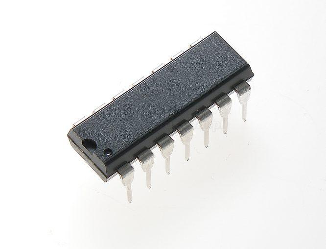
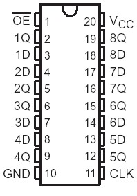
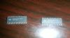
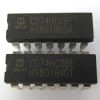
CD74FCT374: Features: BiCMOS Technology With Low Quiescent Power 3-State Outputs Drive Bus Lines DirectlyBuffered InputsNoninverted OutputsInput/Output Isolation From VCCControlled Output Edge Rates48-mA Output...
SeekIC Buyer Protection PLUS - newly updated for 2013!
268 Transactions
All payment methods are secure and covered by SeekIC Buyer Protection PLUS.
The CD74FCT374 is an octal, edge-triggered, D-type flip-flop that uses a small-geometry BiCMOS technology and features 3-state outputs designed specifically for driving highly capacitive or relatively low-impedance loads. This device is particularly suitable for implementing buffer registers, I/O ports, bidirectional bus drivers, and working registers.
The CD74FCT374 output stage is a combination of bipolar and CMOS transistors that limits the output high level to two diode drops below VCC. This CD74FCT374 resultant lowering of output swing (0 V to 3.7 V) reduces power-bus ringing [a source of electromagnetic interference (EMI)] and minimizes VCC bounce and ground bounce and their effects during simultaneous output switching. The output configuration also enhances switching speed and is capable of sinking 48 mA.
The CD74FCT374 eight flip-flops enter data into their registers on the low-to-high transition of the clock (CLK). The output-enable (OE) input controls the 3-state outputs and is independent of the register operation. When OE is high, the outputs are in the high-impedance state.
A buffered OE input can be used to place the eight outputs in either a normal logic state (high or low) or the high-impedance state. In the high-impedance state, the outputs neither load nor drive the bus lines significantly. The CD74FCT374 high-impedance state and the increased drive provide the capability to drive bus lines without interface or pullup components.
OE does not affect internal operations of the flip-flop. Old data can be retained or new data can be entered while the outputs are in the high-impedance state.
To ensure the high-impedance state during power up or power down, OE should be tied to VCC through a pullup resistor; the CD74FCT374 minimum value of the resistor is determined by the current-sinking capability of the driver.
The CD74FCT374 is characterized for operation from 0°C to 70°C.