Features: • Buffered Inputs
• Typical Propagation Delay: 5.6ns at VCC = 5V,
TA = 25oC
• Positive Edge Triggered
• CD74FCT564
- Inverting
• CD74FCT574
- Noninverting
• SCR Latchup Resistant BiCMOS Process and Circuit Design
• Speed of Bipolar FAST™/AS/S
• 48mA Output Sink Current
• Output Voltage Swing Limited to 3.7V at VCC = 5V
• Controlled Output Edge Rates
• Input/Output Isolation to VCC
• BiCMOS Technology with Low Quiescent Power
Pinout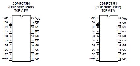 Specifications
Absolute Maximum Ratings Thermal Information
DC Supply Voltage (VCC) . . . . . . . . . . . . . . . . . . . . . . . . -0.5V to 6V
DC Diode Current, IIK (For VI < -0.5V) . . . . . . . . . . . . . . . . . . -20mA
DC Output Diode Current, IOK (for VO < -0.5V) . . . . . . . . . . . -50mA
DC Output Sink Current per Output Pin, IO . . . . . . . . . . . . . . .70mA
DC Output Source Current per Output Pin, IO . . . . . . . . . . . . -30mA
DC VCC Current (ICC) . . . . . . . . . . . . . . . . . . . . . . . . . . . . . .140mA
DC Ground Current (IGND). . . . . . . . . . . . . . . . . . . . . . . . . . .400mA
Operating Conditions
Operating Temperature Range, TA . . . . . . . . . . . . . . . . .0oC to 70oC
Supply Voltage Range, VCC. . . . . . . . . . . . . . . . . . . .4.75V to 5.25V
DC Input Voltage, VI . . . . . . . . . . . . . . . . . . . . . . . . . . . . . . 0 to VCC
DC Output Voltage, VO. . . . . . . . . . . . . . . . . . . . . . . . . . . 0 to VCC
Input Rise and Fall Slew Rate, dt/dv. . . . . . . . . . . . . . . . 0 to 10ns/V
Thermal Resistance (Typical, Note 2) JA (oC/W)
PDIP Package . . . . . . . .. . 135
SOIC Package . . . . . . . . . . 125
SSOP Package . . . . . . . . . . 130
Maximum Junction Temperature . . . . . . . . . . . . . . . . . . . . . . . 150oC
Maximum Storage Temperature Range . . . . . . . . . .-65oC to 150oC
Maximum Lead Temperature (Soldering 10s) . . . . . . . . . . . . . 300oC
(SOIC and SSOP-Lead Tips Only)
CAUTION: Stresses above those listed in "Absolute Maximum Ratings" may cause permanent damage to the device. This is a stress only rating and operation of the device at these or any other conditions above those indicated in the operational sections of this specification is not implied.
NOTE:
2. qJA is measured with the component mounted on an evaluation PC board in free air.
DescriptionThe CD74FCT564 and CD74FCT574 are octal D-Type, three-state, positive edge triggered flip-flops which use a small geometry BiCMOS technology. The CD74FCT564 output stage is a combination of bipolar and CMOS transistors that limits the output HIGH level to two diode drops below VCC. This resultant lowering of output swing (0V to 3.7V) reduces power bus ringing (a source of EMI) and minimizes VCC bounce and ground bounce and their effects during simultaneous output switching. The CD74FCT564 output configuration also enhances switching speed and is capable of sinking 48 milliamperes.
The eight flip-flops enter data into their registers on the LOW to HIGH transition of the clock (CP). The Output Enable (OE) controls the three state outputs and is independent of the register operation. When the Output Enable (OE) is HIGH, the outputs are in the high impedance state. The CD74FCT564 and CD74FCT574 share the same configurations; the CD74FCT564, however, has inverted outputs and the CD74FCT574 has noninverted outputs.

 CD74FCT564 Data Sheet