Features: • Buffered Inputs and Outputs
• Typical Propagation Delay: 13ns (Data to Output at VCC = 5V, CL = 15pF, TA = 25
• Serial or Parallel Expansion Without External Gating
• Fanout (Over Temperature Range)
- Standard Outputs . . . . . . . . . . . . . . . 10 LSTTL Loads
- Bus Driver Outputs . . . . . . . . . . . . . 15 LSTTL Loads
• Wide Operating Temperature Range . . . -55 to 125
• Balanced Propagation Delay and Transition Times
• Significant Power Reduction Compared to LSTTL Logic ICs
• HC Types
- 2V to 6V Operation
- High Noise Immunity: NIL = 30%, NIH = 30%of VCC at VCC = 5V
• HCT Types
- 4.5V to 5.5V Operation
- Direct LSTTL Input Logic Compatibility, VIL= 0.8V (Max), VIH = 2V (Min)
- CMOS Input Compatibility, Il 1µA at VOL, VOHPinout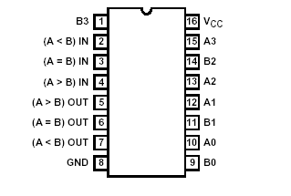 Specifications
DC Supply Voltage, VCC . . . . . . . . . . . . . . . . ..... . . ... . . . . -0.5V to 7V
DC Input Diode Current, IIK
For VI < -0.5V or VI > VCC + 0.5V . . ................................. . .±20mA
DC Output Diode Current, IOK
For VO < -0.5V or VO > VCC + 0.5V . . . . . . . . . . . . . . . . . .... . .±20mA
DC Output Source or Sink Current per Output Pin, IO
For VO > -0.5V or VO < VCC + 0.5V . . . . . . . . . . . . . . . . . .... .. .±25mA
DC VCC or Ground Current, ICC or IGND . . . . . . . . . . . . . . .... . . .±50mA
Temperature Range (TA) . . . . . . . . . . . . . . . . . . ........... . . -55 to 125
Supply Voltage Range, VCC
HC Types . . . . . . . . . . . . . . . . . . . . . . . . . . . . . . . ........... . . . . .2V to 6V
HCT Types . . . . . . . . . . . . . . . . . . . . . . . . . . . . . ........... . . .4.5V to 5.5V
DC Input or Output Voltage, VI, VO . . . . . . . . . . . . ........... . . . . 0V to VCC
Input Rise and Fall Time
2V . . . . . . . . . . . . . . . . . . . . . . . . . . . . . . . . . . . . ........... . 1000ns (Max)
4.5V. . . . . . . . . . . . . . . . . . . . . . . . . . . . . . . . . . ........... . . . 500ns (Max)
6V . . . . . . . . . . . . . . . . . . . . . . . . . . . . . . . . . . . . ........... . . 400ns (Max)
Package Thermal Impedance, JA (see Note 1):
E (PDIP) Package . . . . . . . . . . . . . . . . . . . . . . . . . ............. . . . . .67/W
M (SOIC) Package. . . . . . . . . . . . . . . . . . . . . . . . . ............. . . . . .73/W
NS (SOP) Package . . . . . . . . . . . . . . . . . . . . . . . . . ............... . . . 64/W
PW (TSSOP) Package . . . . . . . . . . . . . . . . . . . . . . ................ . . 108/W
Maximum Junction Temperature . . . . . . . . . . . . . . . . . ............ . . . . . 150
Maximum Storage Temperature Range . . . . . . . ............... . .-65 to 150
Maximum Lead Temperature (Soldering 10s) . . . . . . . . ............ . . . . 300
(SOIC - Lead Tips Only)
CAUTION: Stresses above those listed in "Absolute Maximum Ratings" may cause permanent damage to the
device. This is a stress only rating and operation of the device at these or any other conditions above
those indicated in the operational sections of this specification is not implied.
NOTE: 1. The package thermal impedance is calculated in accordance with JESD 51-7.
DescriptionThe 'HC85 and 'HCT85 are high speed magnitude comparators that use silicon-gate CMOS technology to achieve operating speeds similar to LSTTL with the low power consumption of standard CMOS integrated circuits.
These 4-bit CD74HC85 compare two binary, BCD, or other monotonic codes and present the three possible magnitude results at the outputs (A > B, A < B, and A = B). The 4-bit input words are weighted (A0 to A3 and B0 to B3), where A3
and B3 are the most significant bits.
CD74HC85 are expandable without external gating, in both serial and parallel fashion. The upper part of the truth table indicates operation using a single device or devices in a serially expanded application. The parallel expansion scheme is described by the last three entries in the truth table.

 CD74HC85 Data Sheet