CD74HCT03

Features: • Buffered Inputs• Typical Propagation Delay: 8ns at VCC = 5V,CL = 15pF, TA = 25• Output Pull-up to 10V• Fanout (Over Temperature Range) - Standard Outputs . . . . . . . . . . . . . . . 10 LSTTL Loads - Bus Driver Outputs . . . . . . . . .. . . . . 15 LSTTL Loads&...

product image

CD74HCT03 Picture
SeekIC No. : 004312086 Detail

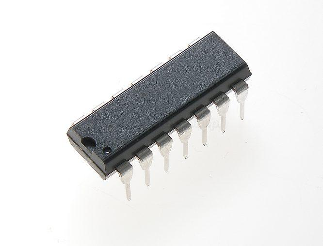
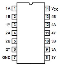
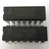
CD74HCT03: Features: • Buffered Inputs• Typical Propagation Delay: 8ns at VCC = 5V,CL = 15pF, TA = 25• Output Pull-up to 10V• Fanout (Over Temperature Range) - Standard Outputs . . . . ...

floor Price/Ceiling Price

Part Number:
CD74HCT03
Supply Ability:
5000

Price Break

  • Qty
  • 1~5000
  • Unit Price
  • Negotiable
  • Processing time
  • 15 Days
Total Cost: $ 0.00

SeekIC Buyer Protection PLUS - newly updated for 2013!

  • Escrow Protection.
  • Guaranteed refunds.
  • Secure payments.
  • Learn more >>

Month Sales

268 Transactions

Rating

evaluate  (4.8 stars)

Upload time: 2024/3/28

Payment Methods

All payment methods are secure and covered by SeekIC Buyer Protection PLUS.

Notice: When you place an order, your payment is made to SeekIC and not to your seller. SeekIC only pays the seller after confirming you have received your order. We will also never share your payment details with your seller.
Product Details

Description


Features:

• Buffered Inputs
• Typical Propagation Delay: 8ns at VCC = 5V,CL = 15pF, TA = 25
• Output Pull-up to 10V
• Fanout (Over Temperature Range)
       - Standard Outputs . . . . . . . . . . . . . . . 10 LSTTL Loads
       - Bus Driver Outputs  . . . . . . . . . . . . . . 15 LSTTL Loads
• Wide Operating Temperature Range  . . . -55oC to 125oC
• Balanced Propagation Delay and Transition Times
• Significant Power Reduction Compared to LSTTL Logic ICs
• HC Types
      - 2V to 6V Operation
      - High Noise Immunity: NIL = 30%, NIH = 30% of VCC at VCC = 5V
• HCT Types
      - 4.5V to 5.5V Operation
      - Direct LSTTL Input Logic Compatibility,VIL= 0.8V (Max), VIH = 2V (Min)
      - CMOS Input Compatibility, Il 1µA at VOL, VOH


Pinout

  Connection Diagram


Specifications

DC Supply Voltage, VCC . . . . . . . . . . . . . . . . . . . . . . . . -0.5V to 7V
DC Input Diode Current, IIK
  For VI < -0.5V or VI > VCC + 0.5V. . . . . . . . . . . . . . . . . . . . . .±20mA
DC Output Diode Current, IOK
  For VO < -0.5V or VO > VCC + 0.5V . . . . . . . . . . . . . . . . . . . .±20mA
DC Output Source or Sink Current per Output Pin, IO
  For VO > -0.5V or VO < VCC + 0.5V . . . . . . . . . . . . . . . . . . . .±25mA
DC Drain Current, per Output, IO
  For -0.5V < VO  . . . . . . . . . . . . . . . . . . . . . . . . . . . . . . . . . . -25mA
DC VCC or Ground Current, ICC or IGND . . . . . . . . . . . . . . . . . .±50mA


Description

The 'HC03 and 'HCT03 logic gates utilize silicon gate CMOS technology to achieve operating speeds similar to LSTTL gates with the low power consumption of standard CMOS integrated circuits. CD74HCT03 have the ability to drive 10 LSTTL loads. The HCT logic family is functionally as well as pin compatible with the standard LS logic family.
These open drain NAND gates can drive into resistive loads to output voltages as high as 10V. CD74HCT03 Minimum values of RL required versus load voltage are shown in Figure 2.


Customers Who Bought This Item Also Bought

Margin,quality,low-cost products with low minimum orders. Secure your online payments with SeekIC Buyer Protection.
Circuit Protection
Cables, Wires
Prototyping Products
DE1
View more