Features: ` Qualification in Accordance With AEC-Q100†` Qualified for Automotive Applications` Customer-Specific Configuration Control Can Be Supported Along With Major-Change Approval` Wide Analog Input Voltage Range:` 5 V Max` Low ON Resistance − 70 Typical (VCC − VEE = 4.5 V)...
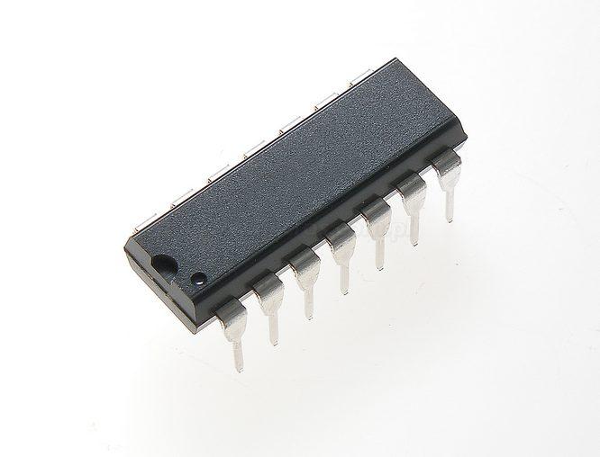
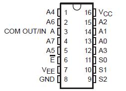
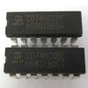
CD74HCT4051-Q1: Features: ` Qualification in Accordance With AEC-Q100†` Qualified for Automotive Applications` Customer-Specific Configuration Control Can Be Supported Along With Major-Change Approval` Wide A...
SeekIC Buyer Protection PLUS - newly updated for 2013!
268 Transactions
All payment methods are secure and covered by SeekIC Buyer Protection PLUS.
Supply voltage range: VCC − VEE (see Note 1) . . . . . . . . −0.5 V to 10.5 V
VCC . . . . . . . . . . . . . . . . . . . . . . . . . . . . . . . . . . . . . . . . . . −0.5 V to +7 V
VEE . . . . . . . . . . . . . . . . . . . . . . . . . . . . . . . . . . . . . . . . . . . . 0.5 V to −7 V
Input clamp current, IIK (VI < −0.5 V or VI > VCC + 0.5 V) . . . . . . ±20 mA
Output clamp current, IOK (VO < VEE − 0.5 V or VO > VCC + 0.5 V)±20 mA
Switch current (VI > VEE − 0.5 V or VI < VCC + 0.5 V) . . . . . . . . . .±25 mA
Continuous current through VCC or GND . . . . . . . . . . . . . . . . . . . ±50 mA
VEE current, IEE . . . . . . . . . . . . . . . . . . . . . . . . . . . . . . . . . . . . . . . −20 mA
Package thermal impedance, JA (see Note 2) . . . . . . . . . . . . . . 73°C/W
Maximum junction temperature, TJ . . . . . . . . . . . . . . . . . . . . . . . . .150°C
Lead temperature (during soldering):
At distance 1/16 ± 1/32 inch (1,59 ± 0,79 mm) from case for 10 s max . 300°C
Storage temperature range, Tstg . . . . . . . . . . . . . . . . . −65°C to 150°C
† Stresses beyond those listed under "absolute maximum ratings" may cause permanent damage to the device. These are stress ratings only, and functional operation of the device at these or any other conditions beyond those indicated under "recommended operating conditions" is not implied. Exposure to absolute-maximum-rated conditions for extended periods may affect device reliability.
NOTES: 1. All voltages referenced to GND unless otherwise specified.
2. The package thermal impedance is calculated in accordance with JESD 51-7.
CD74HCT4051-Q1 is a digitally controlled analog switch that utilizes silicon-gate CMOS technology to achieve operating speeds similar to LSTTL, with the low power consumption of standard CMOS integrated circuits.
This analog multiplexer/demultiplexer controls analog voltages that may vary across the voltage supply range (i.e., VCC to VEE ). CD74HCT4051-Q1 is a bidirectional switch that allows any analog input to be used as an output and vice-versa. The switch has low ON resistance and low OFF leakages. In addition, CD74HCT4051-Q1 has an enable control that, when high, disables all switches to their OFF state.