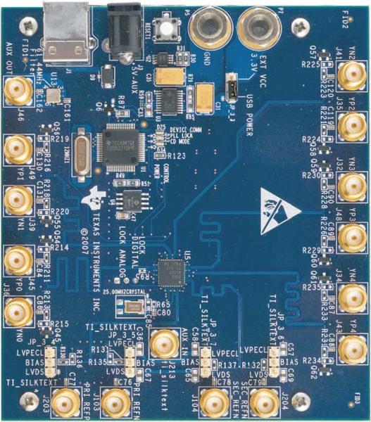
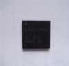
DescriptionThe CDCE18005 is a high performance clock generator and distributor featuring a high degree of configurability via a SPI interface, and programmable start up modes determined by on-board EEPROM.Specifically tailored for buffering clocks for data converters and high-speed digital signals, the CDCE18005 achieves low additive jitter in the 50 fs RMS (1) range. The clock distribution block includes five individually programmable outputs that can be configured to provide different combinations of output formats (LVPECL, LVDS, LVCMOS). Each output can also be programmed to a unique output frequency (up to 1.5 GHz (2)) and skew relationship via a programmable delay block.
Features of the CDCE18005 are:(1)Universal Input Buffers That Accept LVPECL,LVDS, or LVCMOS Level Signaling; (2)Fully Configurable Outputs Including Frequency, Output Format, and Output Skew; (3)Output Multiplexer That Serves as a Clock Switch Between the Three Reference Inputs and the Outputs; (4)Clock Generation Via AT-Cut Crystal; (5)Integrated EEPROM Determines Device Configuration at Power-up; (6)Low Additive Jitter Performance; (7)Universal Output Blocks Support up to 5 Differential, 10 Single-ended, or Combinations of Differential or Single-ended: Low Additive Jitter Output Frequency up to 1.5 GHz LVPECL, LVDS, LVCMOS, and Special High Output Swing Modes Independent Output Dividers Support Divide Ratios from 1 80 Independent limited Coarse Skew Control on all Outputs.
The absolute maximum ratings of the CDCE18005 can be summarized as:(1)Supply voltage range (2) -0.5 to 4.6 V; (2)Input voltage range (3) 0.5 to VCC + 0.5 V; (3)Output voltage range (3) 0.5 to VCC + 0.5 V; (4)Input Current (V I < 0, V I > V CC ) ± 20 mA; (5)Output current for LVPECL/LVCMOS Outputs (0 < V O < V CC) ± 50 mA; (6)Maximum junction temperature 125 ° C; (7)Storage temperature range 65 to 150 ° C.
If you want to know more CDCE18005 information such as the electrical characteristics ,please download the datasheet in www.seekdatasheet.com .

 CDCE18005 Data Sheet