DescriptionThe CDCU2A877 is a high-performance, low-jitter, low-skew, zero-delay buffer that distributes a differential clock input pair (CK, CK ) to 10 differential pairs of clock outputs (Yn, Yn ) and to one differential pair of feedback clock outputs (FBOUT, FBOUT ). The clock outputs are controlled by the input clocks (CK, CK ), the feedback clocks (FBIN, FBIN ), the LVCMOS control pins (OE, OS), and the analog power input (AV DD ). When OE is low, the clock outputs, except FBOUT/ FBOUT , are disabled while the internal PLL continues to maintain its locked-in frequency. OS (output select) is a program pin that must be tied to GND or V DD . When OS is high, OE functions as previously described. When OS and OE are both low, OE has no affect on Y7/ Y7 , they are free running.When AV DD is grounded, the PLL is turned off and bypassed for test purposes.
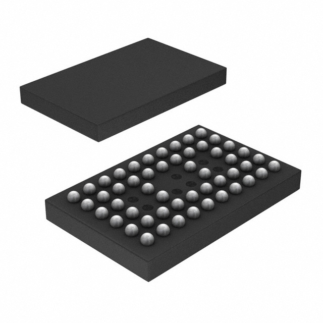
Features of the CDCU2A877 are:(1)1.8-V/1.9-V Phase Lock Loop Clock Driver for Double Data Rate ( DDR II ) Applications; (2)Spread Spectrum Clock Compatible; (3)Operating Frequency: 125 MHz to 410 MHz; (4)Application Frequency: 160 MHz to 410 MHz; (5)Low Jitter (Cycle-Cycle): ± 40 ps; (6)Low Output Skew: 35 ps; (7)Stabilization Time <6 s; (8)Distributes One Differential Clock Input to 10 Differential Outputs; (9)High-Drive Version of CDCUA877; (10)52-Ball mBGA ( MicroStar Junior ? BGA,0,65-mm pitch); (11)External Feedback Pins ( FBIN, FBIN ) are Used to Synchronize the Outputs to the Input Clocks; (12)Meets or Exceeds CUA877/CUA878 Specification PLL Standard for PC2-3200/4300/5300/6400; (13)Fail-Safe Inputs.
The absolute maximum ratings of the CDCU2A877 can be summarized as:(1)Supply voltage range : 0.5 to 2.5 V; (2)Input voltage range (2) (3): 0.5 to V DDQ + 0.5 V; (3)Output voltage range (2) (3): 0.5 to V DDQ + 0.5 V; (4)Input clamp current, (V I < 0 or V I > V DDQ ): ± 50 mA; (5)Output clamp voltage, (V O < 0 or V O > V DDQ ): ± 50 mA; (6)Continuous output current, (V O = 0 to V DDQ ) :± 50 mA; (7)Continuous current through each V DDQ or GND :± 100 mA
If you want to know more CDCU2A877 information such as the electrical characteristics ,please download the datasheet in www.seekdatasheet.com .

 CDCU2A877 Data Sheet