Features: ·Fully programmable frequency generator
·Provides frequencies to 135 MHz
·Configurable high-speed complementary clock outputs
·CMOS output clocks
·Glitch-free transitions for clock changes
·Powers up in a known state
·Single supply (a5V) operation
·Low current draw, ideal for battery applications
·Read/write control register
·Internal VCO and loop filtersPinout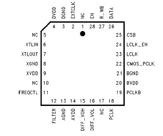 SpecificationsSupply Voltage (VDD) -0.5V to + 6.3V
DC Input Voltage (VIN) -1.5V to VDD + 1.5V
DC Output Voltage (VOUT) -0.5V to VDD + 0.5V
Clamp Diode Current (IIK, IOK) +20 mA
DC Output Current, per pin (IDD) +35 mA
DC VDD or GND Current, per Pin (IDD) +70 mA
Storage Temperature Range (TSTG) -165 to +150
Power Dissipation (PD) 500 mW
Lead Temperature (TL) (Soldering, 10 sec.) 260
Typical JA 0 LFM 50/W
225 LFM 36/W
500 LFM 30/W
900 LFM 29/W
DescriptionThe CGS410 is a programmable clock generator which produces a variable frequency clock output for use in graphics, disk drives and clock synchronizing applications. The CGS410 produces output clocks in CMOS and differential formats. The user is able to program the differential output levels to best suit the levels of the interfacing device. A common configuration allows PCLK to emulate positive ECL logic levels, eliminating the need for TTL to ECL translation.
The CGS410 is referenced off the XTLIN input which can be configured for either external crystal or external oscillator support. All internal frequency generation is referenced from the XTLIN input. The CGS410 can also be driven by EXTCLK as desired. EXTCLK may serve as the source from a fixed clock (for passthru mode), or as an external VCO input.
The CGS410 contains three internal user-selectable low pass filters (LPFs). A fourth option allows for the use of an external LPF configuration. Use of the internal filters greatly simplifies layout, reduces board real estate, and minimizes part count. A programmable polarity charge pump allows the user to optimize the optional external LPF circuitry.
The primary loop structure of the CGS410 consists of programmable N and R dividers. Both are contiguous; N can be any value between 2 and 16383, and R can be any value between 1 and 1023. Additional dividers of the internal VCO allow individual programmability for the PCLK, CMOSPCLK, and LCLK outputs.
An additional advantage of the CGS410 is its ability to perform smooth, glitch-free clock output changes as the user selects passthru clock sources or changes the VCO frequency. A real-time synchronous load clock enable (LCLKEN) control input allows for the enabling and disabling of the LCLK output. This is suitable for applications which require the removal of an active LCLK during the blanking portion of a screen refresh.
On power-up the XTLIN frequency is internally divided by two and routed to the PCLK outputs, providing a known power-up output frequency with a 50% duty cycle. The CGS410 is programmed by a serial stream of data. A serial bit read can verify the contents of the register.

 CGS410 Data Sheet