Features: Very low/programmable power
0.07W @ 5MSPS
0.22W @ 20MSPS
0.40W @ 30MSPS
Single supply operation (+5V)
0.5 LSB differential linearity error
Wide dynamic range
72dBc spurious-free dynamic range
68dB signal-to-noise ratio
No missing codesApplicationCCD imaging
IR imaging
FLIR processing
Medical imaging
High definition video
Instrumentation
Radar processing
Digital communicationsPinout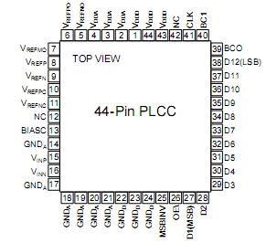 Specificationssupply voltage(VDD) -0.5V to +7V
differential voltage between any two GND's 200m
analog input voltage range -0.5V to +VDD
digital input voltage range -0.5V to +VDD
output short circuit duration (one pin to gnd) infinite
junction temperature +175
storage temperature range -65 to +150
lead solder duration (+300) 10 seDescription The Comlinear CLC949 is a 12-bit analog-to-digital converter sub-system including 12-bit quantizer, sample-and-hold amplifier, and internal reference. The CLC949 has been optimized for low power operation with high dynamic range. The CLC949 has a unique feature which allows the user to adjust internal bias levels in the converter which results in a trade-off between power dissipation and maximum conversion rate. With bias set for 220mW power dissipation the converter operates at 20MSPS. Under these conditions, dynamic performance with a 9.9MHz analog input is typically 68dB SNR and 72dBc SFDR. When bias is set for only 65mW power dissipation the converter maintains excellent perfor-mance at 5MSPS. With a 2.4MHz analog input signal the SNR is 70dB and SFDR is 78dBc. This excellent dynamic performance in the frequency domain without high power requirements make the part a strong performer for communications and radar applications.The low input noise of the CLC949, its 0.5LSB differential linearity error specification, fast settling, and low power dissipation also lead to excellent performance in imaging systems. All parts are thoroughly tested to insure that guaranteed specifications are met.
The CLC949 incorporates an input sample-and-hold amplifier followed by a quantizer which uses a pipelined architecture to min-imize comparator count and the associated power dissipation penalty. An on-board voltage reference is provided. Analog input signals, conversion clock, and a single supply are all that are required for CLC949 operation.
The CLC949 exhibits very stable performance over the commercial and industrial temperature ranges. Most parameters shift very little as the ambient temperature changes from -40°,C to 85°,C. exception to this rule is the dynamic performance of the converter. As the temperature is increased, the distortion increases, especially at higher input frequencies. This can be seen in the plot on page 3. For input frequencies below 7MHz, there is relatively little variation in distortion as the temperature is changed, but at higher input frequencies, it is apparent that the performance degrades as the temperature is increased.
Note that the reason for this degradation is the reduced ability of the CLC949 to handle high slew rates at high temperatures. In applications such as CCD imaging systems, where the slew rate at the A/D sampling instant is very low, this degradation will not be nearly so pronounced.
For applications requiring high temperature operation and very low distortion with high frequency input signals, use of an external sample-and-hold amplifier may enhance performance by reducing the slew rates that the CLC949 sees during its sampling period (just after the falling edge of CLK).
The CLC949 is fabricated in a 0.9m CMOS technology. The Power (mW)CLC949ACQ is specified over the commercial temperature range of 0 to +70 and the CLC949AJQ is specified over the indus-trial range of -40 to +85. Both are packaged in a 44-pin rrier (PLCC)

 CLC949 Data Sheet


