Features: • Direct down-conversion receiver eliminates the external
image reject/IF filters
• Three separate LNAs with single-ended inputs
• RF gain range: GSM = 20 dB, DCS = 22 dB,
PCS = 20 dB. Baseband gain range = 100 dB
• Gain selectable in 2 dB steps
• Integrated receive baseband filters with tunable bandwidth
• Integrated DC offset correction sequencer
• Reduced filtering requirements with translational loop
transmit architecture
• Integrated transmit VCOs
• Wide RF range for quad band operation
• Integrated PAC loop
• Single integrated, fully programmable fractional-N
synthesizer suitable for multi-slot GPRS operation
• Fully integrated wideband Ultra High Frequency (UHF) VCO
• Integrated crystal oscillator
• Separate enable lines for power management transmit,
receive, and synthesizer modes
• Supply voltage down to 2.6 V
• Band select and front-end enable states may be exercised
on output pins to control external circuitry.
• Low external component count
• Optional bypass of baseband filtering for use with high
dynamic range Analog to Digital Converters (ADCs) for
current savings
• Interfaces to low dynamic range ADC
• Meets AM suppression requirements without baseband interaction.
• 56-pin RFLGA 8x8 mm package (low temperature option,
CX74063-34; high temperature option, CX74063-35 and CX74063-36)
• Low power standby modeApplication• GSM850, EGSM900, DCS1800, and PCS1900 handsets
• GPRS handsets and modules
• EDGE downlink supportPinout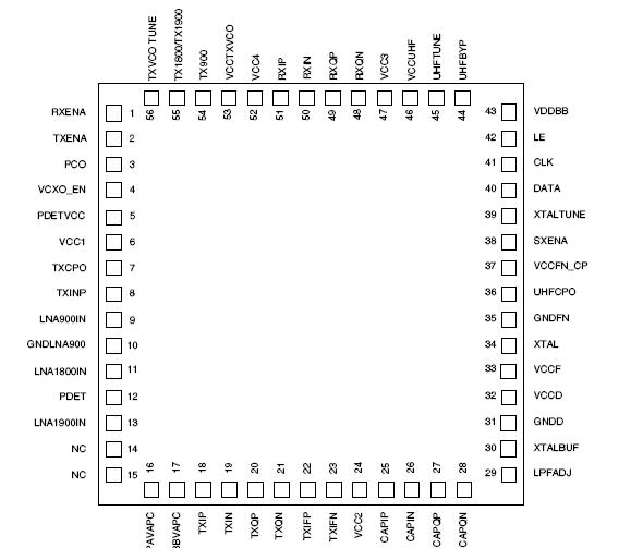 Specifications
| Parameter |
Minimum |
Maximum |
Units |
| Supply voltage (VCC) |
-0.3 |
+3.6 |
V |
| Ambient operating temperature range |
-40 |
+95 |
°C |
| Storage temperature range |
-50 |
+125 |
°C |
| Input voltage range |
GND |
VCC |
V |
| Maximum power dissipation |
|
600 |
mW |
Note: Stresses above these absolute maximum ratings may cause permanent damage. These are
stress ratings only and functional operation at these conditions is not implied. Exposure to
maximum rating conditions for extended periods may reduce device reliability. |
DescriptionThe CX74063-3x transceiver (including 34, -35, and 36 package options) is a highly integrated device for multi-band Global System for Mobile Communications™ (GSM™) or General Packet Radio Service (GPRS) applications. The device requires a minimal number of external components to complete a GSM radio subsystem. The CX74063-3x supports GSM850, EGSM900, DCS1800, and PCS1900 applications. The receiver also supports downlink Enhanced Data-Rate GSM Evolution (EDGE).
The receive path implements a direct down-conversion architecture that eliminates the need for Intermediate Frequency (IF) components. The CX74063-3x receiver consists of three integrated Low Noise Amplifiers (LNAs), a quadrature demodulator, tunable receiver baseband filters, and a DCoffset correction sequencer. In the transmit path, the device consists of an In-phase and Quadrature (I/Q) modulator within a frequency translation loop designed to perform frequency up-conversion with high output spectral purity. This loop also contains a phase-frequency detector, charge pump, mixer, programmable dividers, and high power transmit Voltage Controlled Oscillators (VCOs) with no external tank required. With the integrated gain controller (and an integrator ), the device realizes the Power Amplifier Control (PAC) functionality when combined with a coupler, a Radio Frequency (RF) detector and a Power Amplifier (PA).
The CX74063-3x also features an integrated, fully programmable, sigma-delta fractional-N synthesizer suitable for GPRS multi-slot operation. Except for the loop filter, the frequency synthesizer function, including a wideband VCO, is completely on-chip. The reference frequency for the synthesizer is supplied by the integrated crystal oscillator circuitry.
CX74063-3x 56-pin 8x8 RF Land Grid Array (RFLGA™) device package and pin configuration are shown in Figure 1. A functional block diagram is shown in Figure 2. Signal pin assignments, functional pin descriptions, and equivalent circuitry are provided in Table 1.

 CX74063-3x Data Sheet