Features: • A wide instruction set (213 instructions) which cover various types of data
- 16-bit arithmetic instruction/multiplication and division instructions/boolean bit operation instruction
• Minimum instruction cycle During operation 250ns/16MHz, During operation 122µs/32kHz
• Incorporated ROM capacity 32Kbytes (CXP88132), 40Kbytes (CXP88140)
• Incorporated RAM capacity 1296bytes
• Peripheral function
- A/D converter 8-bit, 8-channel, successive approximation system (Conversion time: 20.0µs/16MHz)
- Serial I/O with auto transfer mode Incorporated 8-stage FIFO for data (1 to 8 bytes auto transfer)
- Timer 8-bit timer/counter, 2-channel, 19-bit time base timer
- High precision timing pattern generation PPG 8 pins 32-stage programmable circuit RTG 5 pins 2-channel
- PWM/DA gate output 12-bit, 2-channel (Repetitive frequency 62.5kHz/16MHz)
- Servo input control Capstan FG, Drum FG/PG, CTL input
- VSYNC separator
- FRC capture unit Incorporated 26-bit and 8-stage FIFO
- PWM output for tuner 14-bit
- VISS/VASS circuit Pulse duty auto detection circuit
- 32kHz timer/event counter 32kHz oscillation circuit, ultra-low speed instruction mode
- Remote control receiving circuit 8-bit pulse measuring counter, 6-stage FIFO
- FDP controller/driver Max.148 segments can be displayed Hardware key scanning function (Max.16 ´ 3 key matrix available)
- Tri-state output PPG 1 pin, RTG 1 pin, output 8 pins
- Pseudo HSYNC output function
- High speed head switching circuit
• Interruption 22 factors, 15 vectors, multi-interruption possible
• Standby mode SLEEP/STOP
• Package 100-pin plastic QFP
• Piggyback/evaluation chip CXP88100Pinout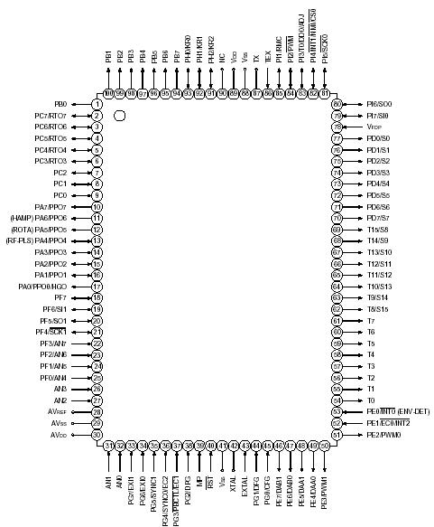 Specifications
| Item |
Symbol |
Rating |
Unit |
Remarks |
| Supply voltage |
VDD |
0.3 to +7.0 |
V |
|
| AVDD |
AVss to +7.0*1 |
V |
|
| AVSS |
0.3 to +0.3 |
V |
|
| Input voltage |
VIN |
0.3 to +7.0*2 |
V |
|
| Output voltage |
VOUT |
0.3 to +7.0*2 |
V |
|
| Display output voltage |
VOD |
VDD 4.0 to VDD + 0.3 |
V |
As P-channel transistor is open drain,
VDD is reference. |
| High level output current |
IOH |
5 |
mA |
All pins excluding display outputs
(value per pin)*3 |
| IODH1 |
15 |
mA |
Display outputs S0 to S7 (value per pin) |
| IODH2 |
35 |
mA |
Display outputs T0 to T7,
and T8/S15 to T15/S8 (value per pin) |
| High level total output current |
IOH |
50 |
mA |
Total for all pins excluding display outputs |
| IODH |
100 |
mA |
Total for all display outputs |
| Low level output current |
IOL |
15 |
mA |
|
| Low level total output current |
IOL |
130 |
mA |
Total for all outputs |
| Operating temperature |
Topr |
20 to +75 |
°C |
|
| Storage temperature |
Tstg |
55 to +150 |
°C |
|
| Allowable power dissipation |
PD |
600 |
mW |
|
DescriptionThe CXP88140 is a CMOS 8-bit microcomputer which consists of A/D converter, serial interface, timer/counter, time base timer, vector interruption, high precision timing pattern generation circuits, PWM generator, PWM for tuner, VISS/VASS circuit, 32kHz timer/event counter, remote control receiving circuit, FDP controller/driver, VCR vertical sync separation circuit and the measuring circuit which measure signals of capstan FG and drum FG/PG and other servo systems, as well as basic configurations like 8-bit CPU, ROM, RAM and I/O port. They are integrated into a single chip.
Also, CXP88140 provides sleep/ stop function which enables to lower power consumption and ultra-low speed instruction mode in 32kHz operation.

 CXP88140 Data Sheet