CXP88740

Features: • A wide instruction set (213 instructions) which cover various types of data- 16-bit arithmetic/multiplication and division/boolean bit operation instructions• Minimum instruction cycle 250ns at 16MHz operation 122µs at 32kHz operation• Incorporated ROM capacity ...

product image

CXP88740 Picture
SeekIC No. : 004319046 Detail

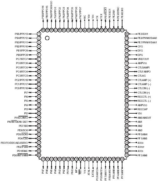
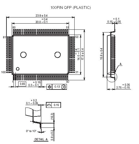
CXP88740: Features: • A wide instruction set (213 instructions) which cover various types of data- 16-bit arithmetic/multiplication and division/boolean bit operation instructions• Minimum instruc...

floor Price/Ceiling Price

Part Number:
CXP88740
Supply Ability:
5000

Price Break

  • Qty
  • 1~5000
  • Unit Price
  • Negotiable
  • Processing time
  • 15 Days
Total Cost: $ 0.00

SeekIC Buyer Protection PLUS - newly updated for 2013!

  • Escrow Protection.
  • Guaranteed refunds.
  • Secure payments.
  • Learn more >>

Month Sales

268 Transactions

Rating

evaluate  (4.8 stars)

Upload time: 2024/5/1

Payment Methods

All payment methods are secure and covered by SeekIC Buyer Protection PLUS.

Notice: When you place an order, your payment is made to SeekIC and not to your seller. SeekIC only pays the seller after confirming you have received your order. We will also never share your payment details with your seller.
Product Details

Description


Features:

• A wide instruction set (213 instructions) which cover various types of data
- 16-bit arithmetic/multiplication and division/boolean bit operation instructions
• Minimum instruction cycle 250ns at 16MHz operation 122µs at 32kHz operation
• Incorporated ROM capacity 32K bytes (CXP88732) 40K bytes (CXP88740) 48K bytes (CXP88748)
• Incorporated RAM capacity 1344 bytes (including PPG RAM)
• Peripheral function
- A/D converter 8 bits, 14 channels, successive approximation system (Conversion time of 20µs/16MHz)
- Serial interface Incorporated 8-bit, 8-stage FIFO for data (Auto transfer for 1 to 8 bytes), 1 channel 8-bit clock sync type, 1 channel
- Timer 8-bit timer/counter, 2 channels 19-bit time base timer 32kHz timer/counter
- High precision timing pattern generation PPG 19 pins 32-stage programmable circuit RTG 5 pins, 1 channel 5-bit, 8-satge FIFO (RECCTL control), 1channel
- PWM/DA gate output 12 bits, 2 channels (Repetitive frequency 62.5kHz/16MHz) DA gate pulse output, 13 bits, 2 channels
- Analog signal input circuit Capstan FG amplifier circuit Drum FG amplifier circuit Drum PG amplifier circuit PBCTL amplifier circuit
- CTL write/rewrite circuit Recording current control circuit
- Servo input control Capstan FG, Drum FG/PG, CTL input
- VSYNC separator
- FRC capture unit Incorporated 26-bit and 8-stage FIFO
- PWM output 14-bit, 1 channel
- VISS/VASS circuit Pulse duty auto detection circuit
- 32kHz timer/event counter 32kHz oscillation circuit, ultra-low speed instruction mode
- Remote control reception circuit 8-bit pulse measurement counter, 6-stage FIFO
- Tri-state output PPG 1 pin, output 8 pins
- Pseudo HSYNC output function
- High speed head switching circuit
• Interruption 20 factors, 15 vectors, multi-interruption possible
• Standby mode SLEEP/STOP
• Package 100-pin plastic QFP
• Piggyback/evaluation chip CXP88800 100-pin ceramic QFP


Pinout

  Connection Diagram

  Connection Diagram

  Connection Diagram


Specifications

  Item Symbol Rating Unit Remarks
  Supply voltage VDD 0.3 to +7.0 V  
AVDD AVss to +7.0*1 V  
AVSS 0.3 to +0.3 V  
AMPVDD AMPVSS to +7.0*2 V  
AMPVSS 0.3 to +0.3 V  
  Input voltage VIN 0.3 to +7.0*3 V  
  Output voltage VOUT 0.3 to +7.0*3 V  
  Medium drive output voltage VOUTP 0.3 to +15.0 V Port H (PH7 to PH4) pin
  High level output current IOH 5 mA  
  High level total output current IOH 50 mA Total of output pins
  Low level output current IOL 15 mA Other than large current output
ports (value per pin)
IOLC 20 mA Large current output port*4
(value per pin)
  Low level total output current IOL 130 mA Total of output pins
  Operating temperature Topr 20 to +75 °C  
  Storage temperature Tstg 55 to +150 °C  
  Allowable power dissipation PD 600 mW QFP package type


Description

The CXP88740 is a CMOS 8-bit microcomputer which consists of A/D converter, serial interface, timer/counter, time base timer, high precision timing pattern generation circuits, PWM output, VISS/ VASS circuit, 32kHz timer/counter, remote control receiving circuit, VSYNC separator and the measurement circuit which measure signals of capstan FG amplifier and drum FG/PG amplifier and other servo systems, as well as basic configurations like 8-bit CPU, ROM, RAM and I/O port. They are integrated into a single chip.
Also, CXP88740 provides sleep/stop function which enables to lower power consumption.


Customers Who Bought This Item Also Bought

Margin,quality,low-cost products with low minimum orders. Secure your online payments with SeekIC Buyer Protection.
Semiconductor Modules
Batteries, Chargers, Holders
Fans, Thermal Management
Crystals and Oscillators
Isolators
Cables, Wires
View more