Features: • A wide instruction set (213 instructions) which cover various types of data
- 16-bit arithmetic/multiplication and division/boolean bit operation instructions
• Minimum instruction cycle 250ns at 16MHz operation 122µs at 32kHz operation
• Incorporated PROM capacity 60K bytes
• Incorporated RAM capacity 1600 bytes (including PPG RAM)
• Peripheral function
- A/D converter 8 bits, 8 channels, successive approximation system (Conversion time of 20µs/16MHz)
- Serial interface Incorporated 8-bit, 8-stage FIFO for data (Auto transfer for 1 to 8 bytes), 1 channel 8-bit clock sync type, 1 channel
- Timer 8-bit timer/counter, 2 channels 19-bit time base timer 32kHz timer/counter
- High precision timing pattern generation PPG 19 pins 32-stage programmable circuit RTG 5 pins, 1 channel 5-bit, 8-satge FIFO (RECCTL control), 1channel
- PWM/DA gate output 12 bits, 2 channels (Repetitive frequency 62.5kHz/16MHz) DA gate pulse output, 13 bits, 2 channels
- Analog signal input circuit Capstan FG amplifier circuit Drum FG amplifier circuit Drum PG amplifier circuit PBCTL amplifier circuit
- CTL write/rewrite circuit Recording current control circuit
- Servo input control Capstan FG, Drum FG/PG, CTL input
- VSYNC separator
- FRC capture unit Incorporated 26-bit and 8-stage FIFO
- PWM output 14-bit, 1 channel
- VISS/VASS circuit Pulse duty auto detection circuit
- 32kHz timer/event counter 32kHz oscillation circuit, ultra-low speed instruction mode
- Remote control reception circuit 8-bit pulse measurement counter, 6-stage FIFO
- Tri-state output PPG 1 pin, output 8 pins
- Pseudo HSYNC output function
- High speed head switching circuit
• Interruption 20 factors, 15 vectors, multi-interruption possible
• Standby mode SLEEP/STOP
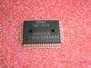
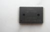
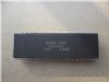
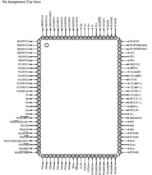
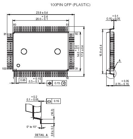
• Package 100-pin plastic QFPPinout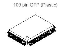
Specifications
| |
Item |
Symbol |
Rating |
Unit |
Remarks |
| |
Supply voltage |
VDD |
0.3 to +7.0 |
V |
|
| AVDD |
AVss to +7.0*1 |
V |
|
| AVSS |
0.3 to +0.3 |
V |
|
| AMPVDD |
AMPVSS to +7.0*2 |
V |
|
| AMPVSS |
0.3 to +0.3 |
V |
|
| |
Input voltage |
VIN |
0.3 to +7.0*3 |
V |
|
| |
Output voltage |
VOUT |
0.3 to +7.0*3 |
V |
|
| |
Medium drive output voltage |
VOUTP |
0.3 to +15.0 |
V |
Port PH |
| |
High level output current |
IOH |
5 |
mA |
|
| |
High level total output current |
IOH |
50 |
mA |
Total of output pins |
| |
Low level output current |
IOL |
15 |
mA |
Other than large current output
ports (value per pin) |
| IOLC |
20 |
mA |
Large current output port*4
(value per pin) |
| |
Low level total output current |
IOL |
130 |
mA |
Total of output pins |
| |
Operating temperature |
Topr |
20 to +75 |
°C |
|
| |
Storage temperature |
Tstg |
55 to +150 |
°C |
|
| |
Allowable power dissipation |
PD |
600 |
mW |
QFP package type |
DescriptionThe CXP888P60 is a CMOS 8-bit micro-computer which consists of A/D converter, serial interface, timer/counter, time base timer, high precision timing pattern generation circuits, PWM output, VISS/VASS circuit, 32kHz timer/counter, remote control receiving circuit, VSYNC separator and the measurement circuit which measure signals of capstan FG amplifier and drum FG/PG amplifier and other servo systems, as well as basic configurations like 8-bit CPU, PROM, RAM and I/O port. They are
integrated into a single chip.
Also, CXP888P60 provides sleep/stop function which enables to lower power consumption. The CXP888P60 is the PROM-incorporated version of the CXP88860 with built-in mask ROM.
This provides the additional feature of being able to write directly into the program. Thus, it is most suitable for evaluation use during system development and for small-quantity production.

 CXP888P60 Data Sheet