CY2PD817

Features: • DC to 320-MHz operation• 50-ps output-output skew• 30-ps cycle-cycle jitter• 2.5V power supply• LVPECL input @ 320-MHz Operation• One LVPECL output @ 320-MHz Operation• Four LVCMOS/LVTTL outputs @ 250 MHz/160 MHz• Two LVCMOS/LVTTL outputs...

product image

CY2PD817 Picture
SeekIC No. : 004319296 Detail

CY2PD817: Features: • DC to 320-MHz operation• 50-ps output-output skew• 30-ps cycle-cycle jitter• 2.5V power supply• LVPECL input @ 320-MHz Operation• One LVPECL output @ ...

floor Price/Ceiling Price

Part Number:
CY2PD817
Supply Ability:
5000

Price Break

  • Qty
  • 1~5000
  • Unit Price
  • Negotiable
  • Processing time
  • 15 Days
Total Cost: $ 0.00

SeekIC Buyer Protection PLUS - newly updated for 2013!

  • Escrow Protection.
  • Guaranteed refunds.
  • Secure payments.
  • Learn more >>

Month Sales

268 Transactions

Rating

evaluate  (4.8 stars)

Upload time: 2024/4/27

Payment Methods

All payment methods are secure and covered by SeekIC Buyer Protection PLUS.

Notice: When you place an order, your payment is made to SeekIC and not to your seller. SeekIC only pays the seller after confirming you have received your order. We will also never share your payment details with your seller.
Product Details

Description


Features:

• DC to 320-MHz operation
• 50-ps output-output skew
• 30-ps cycle-cycle jitter
• 2.5V power supply
• LVPECL input @ 320-MHz Operation
• One LVPECL output @ 320-MHz Operation
• Four LVCMOS/LVTTL outputs @ 250 MHz/160 MHz
• Two LVCMOS/LVTTL outputs @ 250 MHz/80 MHz
• 45% to 55% output duty cycle
• Output divider control
• Output enable/disable control
• Operating temperature range: 0°C to +85°C
• 24-pin TSSOP


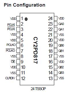
Pinout

  Connection Diagram


Specifications

Parameter Description Condition
Min.
Max.
Unit
VDD DC Supply Voltage  
3.3
V
VDD DC Operating Voltage Functional
2.625
V
VIN DC Input Voltage Relative to VSS, with or VDD applied
VDD + 0.5
V
VOUT DC Output Voltage Relative to VSS
VDD + 0.5
V
VTT Output termination Voltage LVCMOS outputs
VDD / 2
V
LVPECL output
VDD 2
LU Latch Up Immunity Functional
200
mA
RPS Power Supply Ripple Ripple Frequency < 100 kHz
150
mVp-p
TS Temperature, Storage Non-functional
65
+150
°C
TA Temperature, Operating Ambient Functional
0
+85
°C
TJ Temperature, Junction Functional
+150
°C
ØJC Dissipation, Junction to Case Functional
42
°C/W
ØJA Dissipation, Junction to Ambient Functional
105
°C/W
ESDH ESD Protection (Human Body Model)  
2000
V
FIT Failure in Time Manufacturing test
10
ppm
Notes:
1. PU = Internal pull up, PD = Internal pull down.
2. A 0.1-uF bypass capacitor should be placed as close as possible to each positive power pin (< 0.2"). If these bypass capacitors are not close to the pins their high frequency filtering characteristics will be cancelled by the lead inductance of the trace.


Description

The CY2PD817 is a low-voltage LVPECL-to-LVPECL and LVCMOS fanout buffer designed for servers, data communications, and clock management.

The CY2PD817 is ideal for applications requiring mixed differential and single-ended clock distribution. This device accepts an LVPECL input reference clock and provides one LVPECL and six LVCMOS/LVTTL output clocks. The outputs are partitioned into three banks of one, two, and four outputs. The LVPECL output is a buffered copy of the input clock while the LVCMOS outputs are divided by 1, 2, and 4. When CLRDIV is set HIGH, the output dividers are set to 1. In this mode, the maximum input frequency is limited to 250 MHz.

When OE is set HIGH, the outputs are disabled in a High-Z state.


Customers Who Bought This Item Also Bought

Margin,quality,low-cost products with low minimum orders. Secure your online payments with SeekIC Buyer Protection.
Potentiometers, Variable Resistors
Cables, Wires
Undefined Category
Batteries, Chargers, Holders
Sensors, Transducers
View more