CY62126DV30

Features: • Very high speed: 45 ns• Wide voltage range: 2.2V to 3.6V• Pin compatible with CY62126BV• Ultra-low active power- Typical active current: 0.85 mA @ f = 1 MHz- Typical active current: 5 mA @ f = fMAX• Ultra-low standby power• Easy memory expansion with...

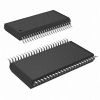
product image

CY62126DV30 Picture
SeekIC No. : 004319377 Detail

CY62126DV30: Features: • Very high speed: 45 ns• Wide voltage range: 2.2V to 3.6V• Pin compatible with CY62126BV• Ultra-low active power- Typical active current: 0.85 mA @ f = 1 MHz- Typi...

floor Price/Ceiling Price

Part Number:
CY62126DV30
Supply Ability:
5000

Price Break

  • Qty
  • 1~5000
  • Unit Price
  • Negotiable
  • Processing time
  • 15 Days
Total Cost: $ 0.00

SeekIC Buyer Protection PLUS - newly updated for 2013!

  • Escrow Protection.
  • Guaranteed refunds.
  • Secure payments.
  • Learn more >>

Month Sales

268 Transactions

Rating

evaluate  (4.8 stars)

Upload time: 2024/4/24

Payment Methods

All payment methods are secure and covered by SeekIC Buyer Protection PLUS.

Notice: When you place an order, your payment is made to SeekIC and not to your seller. SeekIC only pays the seller after confirming you have received your order. We will also never share your payment details with your seller.
Product Details

Description


Features:

• Very high speed: 45 ns
• Wide voltage range: 2.2V to 3.6V
• Pin compatible with CY62126BV
• Ultra-low active power
- Typical active current: 0.85 mA @ f = 1 MHz
- Typical active current: 5 mA @ f = fMAX
• Ultra-low standby power
• Easy memory expansion with CE and OE features
• Automatic power-down when deselected
• Packages offered in a 48-ball FBGA and a 44-lead TSOP Type II
• Also available in Lead-free packages


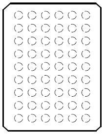
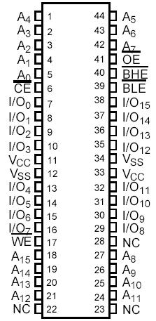
Pinout

  Connection Diagram


Specifications

Storage Temperature .................................65°C to +150°C
Ambient Temperature with
Power Applied.............................................55°C to +125°C
Supply Voltage to Ground
Potential ............................................................. −0.3V to 3.9V
DC Voltage Applied to Outputs
in High-Z State[5.] .....................................−0.3V to VCC + 0.3V
DC Input Voltage[5] .................................. −0.3V to VCC + 0.3V
Output Current into Outputs (LOW)................................. 20 mA
Static Discharge Voltage............................................... > 2001V
(per MIL-STD-883, Method 3015)
Latch-up Current .........................................................> 200 mA


Description

The CY62126DV30 is a high-performance CMOS static RAM organized as 64K words by 16 bits. This device features advanced circuit design to provide ultra-low active current.
This is ideal for providing More Battery Life™ (MoBL®) in portable applications such as cellular telephones. The device also has an automatic power-down feature that significantly reduces power consumption by 90% when addresses are not toggling. The device can be put into standby mode reducing power consumption by more than 99% when deselected (CEHIGH). The input/output pins (I/O0 through I/O15) CY62126DV30 are placed in a high-impedance state when: deselected (CE HIGH),outputs are disabled (OE HIGH), both Byte High Enable and Byte Low Enable are disabled (BHE, BLE HIGH) or during a write operation (CE LOW and WE LOW). Writing to the device is accomplished by taking Chip Enable (CE ) and Write Enable (WE ) inputs LOW. If Byte Low Enable (BLE) is LOW, then data from I/O pins (I/O0 through I/O7), is written into the location specified on the address pins (A0 through A15). If Byte High Enable (BHE) is LOW, then data from I/O pins (I/O8 through I/O15) is written into the location specified on the address pins (A0 through A15). Reading from the device is accomplished by taking Chip Enable (CE ) and Output Enable (OE ) LOW while forcing the Write Enable (WE) HIGH. If Byte Low Enable (BLE ) is LOW,then data from the memory location specified by the address pins will appear on I/O0 to I/O7. If Byte High Enable (BLE) CY62126DV30 is LOW, then data from memory will appear on I/O8 to I/O15. See the truth table at the back of this data sheet for a complete description of read and write modes.


Customers Who Bought This Item Also Bought

Margin,quality,low-cost products with low minimum orders. Secure your online payments with SeekIC Buyer Protection.
Optical Inspection Equipment
Discrete Semiconductor Products
Hardware, Fasteners, Accessories
Semiconductor Modules
Transformers
Potentiometers, Variable Resistors
View more