Features: • Very high speed: 55 ns
• Voltage range: 1.65V to 1.95V
• Ultra-low active power
-Typical active current: 0.5 mA @ f = 1 MHz
-Typical active current: 2.5 mA @ f = fMAX
• Ultra-low standby power
• Easy memory expansion withCE1, , CE2, and OE, features
• Automatic power-down when deselected
• CMOS for optimum speed/power
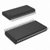
• Packages offered in a 48-ball FBGA and a 44-pin TSOP Type IIPinout SpecificationsStorage Temperature .................................65°C to +150°C
Ambient Temperature with
Power Applied............................................. 55°C to +125°C
Supply Voltage to Ground Potential
.............................................................−0.2V to VCCMAX + 0.2V
DC Voltage Applied to Outputs
in High-Z State[3] .......................................−0.2V to VCC + 0.2V
DC Input Voltage[3] ................................... −0.2V to VCC + 0.2V
Output Current into Outputs (LOW).................................. 20 mA
Static Discharge Voltage................................................ > 2001V
(per MIL-STD-883, Method 3015)
Latch-up Current ......................................................... > 200 mADescriptionThe CY62127DV18 is a high-performance CMOS static RAM organized as 64K words by 16 bits. This device features advanced circuit design to provide ultra-low active current. This is ideal for providing More Battery Life (MoBL®) in portable applications such as cellular telephones. The device also has an automatic power-down feature that significantly reduces power consumption by 99% when addresses are not toggling.
The CY62127DV18 can be put into standby mode reducing power consumption by more than 99% when deselected Chip Enable 1 (CE1 ) HIGH or Chip Enable 2 (CE2 ) LOW or both BHE andBLE are HIGH. The input/output pins (I/O0 through I/O15) are placed in a high-impedance state when: deselected Chip Enable 1 (CE1) HIGH or Chip Enable 2 (CE2) LOW, outputs are disabled (OE HIGH), both Byte High Enable and Byte Low Enable are disabled (BHE, BLE HIGH) or during a write operation (Chip Enable 1 (CE1) LOW and Chip Enable 2 (CE2) HIGH and WE LOW).
Writing to the device is accomplished by taking Chip Enable (CE1) LOW and Chip Enable 2 (CE2) HIGH and Write Enable (WE) input LOW. If Byte Low Enable (BLE) is LOW, then data from I/O pins (I/O0 through I/O7), is written into the location specified on the address pins (A0 through A15). If Byte High Enable (BLE) is LOW, then data from I/O pins (I/O8 through I/O15) is written into the location specified on the address pins(A0 through A15).
Reading from the CY62127DV18 is accomplished by taking Chip Enable 1 (CE1) LOW and Chip Enable 2 (CE2) HIGH and Output Enable (OE) LOW while forcing the Write Enable (WE) HIGH. If Byte Low Enable (BLE) is LOW, then data from the memory location specified by the address pins will appear on I/O0 I/O7. If Byte High Enable (BLE)) is LOW, then data CY62127DV18 from memory will appear on I/O8 to I/O15. See the truth table at the back of this data sheet for a complete description of read and write modes.

 CY62127DV18 Data Sheet