Features: • Temperature Ranges
-Industrial: 40°C to 85°C
-Automotive: 40°C to 125°C (Preliminary)
• Very high speed: 45 ns, 55 ns and 70 ns
• Wide voltage range: 2.20V 3.60V
• Pin-compatible with CY62157CV25, CY62157CV30, and CY62157CV33
• Ultra-low active power
- Typical active current: 1.5 mA @ f = 1 MHz
- Typical active current: 12 mA @ f = fmax
• Ultra-low standby power
• Easy memory expansion with CE1, CE2, and OE features
• Automatic power-down when deselected
• CMOS for optimum speed/power
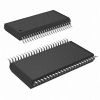
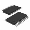
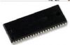
• Packages offered: 48-ball BGA, 48-pin TSOPI, and 44-pin TSOPIIPinout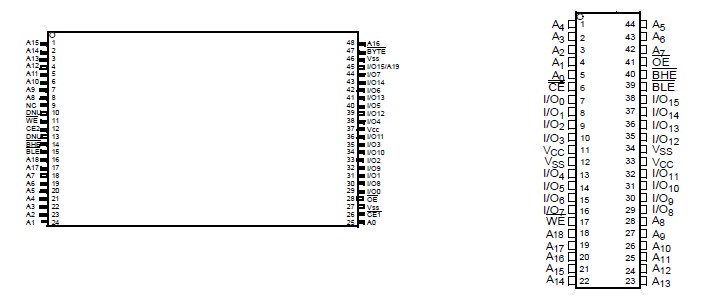 Description
The CY62157DV30 is a high-performance CMOS static RAM organized as 512K words by 16 bits. This device features advanced circuit design to provide ultra-low active current. This is ideal for providing More Battery Life (MoBL®) in portable applications such as cellular telephones.The device also has an automatic power-down feature that significantly reduces power consumption. The CY62157DV30 can also be put into standby mode when deselected (
CE1 HIGH or
CE2 LOW or both
BHE and
BLE are HIGH). The input/output pins of CY62157DV30 (I/O0 through I/O15) are placed in a high-impedance state when: deselected (
CE1 HIGH or
CE2 LOW), outputs are disabled (OE HIGH), both Byte High Enable and Byte Low Enable are
disabled (
BHE,
BLE HIGH), or during a write operation (
CE1 LOW,
CE2 HIGH and WE LOW).
Writing to the CY62157DV30 is accomplished by taking Chip Enables (
CE1 LOW and
CE2 HIGH) and Write Enable (
WE) input LOW. If Byte Low Enable (
BLE) is LOW, then data from I/O pins (I/O0 through I/O7), is written into the location specified on the address pins (A0 through A18). If Byte High Enable (
BHE) is LOW, then data from I/O pins (I/O8 through I/O15) is written into the location specified on the address pins (A0 through A18).
Reading from the CY62157DV30 is accomplished by taking Chip Enables (
CE1 LOW and
CE2 HIGH) and Output Enable (
OE) LOW while forcing the Write Enable (
WE) HIGH. If Byte Low Enable (
BLE) is LOW, then data from the memory location specified by the address pins will appear on I/O0 to I/O7. If Byte High Enable (
BHE) is LOW, then data of CY62157DV30 from memory will appear on I/O8 to I/O15. See the truth table for a complete description of read and write modes.

 CY62157DV30 Data Sheet