Features: * 55, 70 ns access times
* CMOS for optimum speed/power
* Easy memory expansion with CE1, CE2 , and OE fea- tures
* TTL-compatible inputs and outputs
* Automatic power-down when deselectedPinout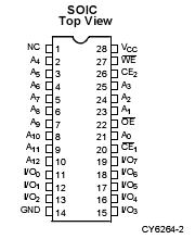 SpecificationsStorage Temperature .................................65°C to +150°C
Ambient Temperature with
Power Applied.............................................55°C to +125°C
Supply Voltage to Ground Potential..................0.5V to +7.0V
DC Voltage Applied to Outputs
in High Z State[1] ............................................0.5V to +7.0V
DC Input Voltage[1].........................................0.5V to +7.0V
Electrical Characteristics Over the Operating Range
Output Current into Outputs (LOW) .............................20 mA
Static Discharge Voltage .......................................... >2001V
(per MIL-STD-883, Method 3015)
Latch-Up Current .................................................... >200 mADescriptionThe CY6264 is a high-performance CMOS static RAM orga- nized as 8192 words by 8 bits. Easy memory expansion is
provided by an active LOW chip enable (CE
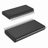
1 ), an active HIGH chip enable (CE2), and active LOW output enable (OE) and three-state drivers. Both devices have an automatic pow-er-down feature (CE1), reducing the power consumption by over 70% when deselected. The CY6264 is packaged in a 450-mil (300-mil body) SOIC.
An active LOW write enable signal (WE) controls CY6264 the writ- ing/reading operation of the memory. When CE
1 and WE in-puts are both LOW and CE
2 is HIGH, data on the eight data input/output pins (I/O
0through I/O
7 ) is written into the memory location addressed by the address present on the address pins (A
0 through A
12). Reading the CY6264 is accomplished by selecting the CY6264 and enabling the outputs, CE
1 and OE active LOW, CE2 active HIGH, while WE remains inactive or HIGH. Under these conditions, the contents of the location ad- dressed by the information on address pins is present on the eight data input/output pins.
The input/output pins of CY6264 remain in a high-impedance state unless the chip is selected, outputs are enabled, and write enable (WE) is HIGH. A die coat is used to insure alpha immunity.

 CY6264 Data Sheet