CY74FCT2541

Features: ` Function and Pinout Compatible With FCT and F Logic` 25- Output Series Resistors to Reduce Transmission-Line Reflection Noise` Reduced VOH (Typically = 3.3 V) Versions of Equivalent FCT Functions` Edge-Rate Control Circuitry for Significantly Improved Noise Characteristics` Ioff S...

product image

CY74FCT2541 Picture
SeekIC No. : 004319528 Detail

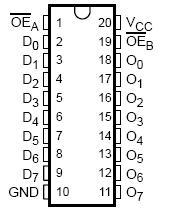
CY74FCT2541: Features: ` Function and Pinout Compatible With FCT and F Logic` 25- Output Series Resistors to Reduce Transmission-Line Reflection Noise` Reduced VOH (Typically = 3.3 V) Versions of Equivalent F...

floor Price/Ceiling Price

Part Number:
CY74FCT2541
Supply Ability:
5000

Price Break

  • Qty
  • 1~5000
  • Unit Price
  • Negotiable
  • Processing time
  • 15 Days
Total Cost: $ 0.00

SeekIC Buyer Protection PLUS - newly updated for 2013!

  • Escrow Protection.
  • Guaranteed refunds.
  • Secure payments.
  • Learn more >>

Month Sales

268 Transactions

Rating

evaluate  (4.8 stars)

Upload time: 2024/4/18

Payment Methods

All payment methods are secure and covered by SeekIC Buyer Protection PLUS.

Notice: When you place an order, your payment is made to SeekIC and not to your seller. SeekIC only pays the seller after confirming you have received your order. We will also never share your payment details with your seller.
Product Details

Description


Features:

` Function and Pinout Compatible With FCT and F Logic
` 25- Output Series Resistors to Reduce
   Transmission-Line Reflection Noise
` Reduced VOH (Typically = 3.3 V) Versions
   of Equivalent FCT Functions
` Edge-Rate Control Circuitry for
   Significantly Improved Noise Characteristics
` Ioff Supports Partial-Power-Down Mode Operation
` ESD Protection Exceeds JESD 22
2000-V Human-Body Model (A114-A)
200-V Machine Model (A115-A)
1000-V Charged-Device Model (C101)
` Matched Rise and Fall Times
` Fully Compatible With TTL Input and
   Output Logic Levels
` 12-mA Output Sink Current
   15-mA Output Source Current
` 3-State Outputs


Pinout

  Connection Diagram


Specifications

Supply voltage range to ground potential . . . . . . . . . . . . . . . . . . . . . . . . . . . . . . . . . . . . . . . . . 0.5 V to 7 V
DC input voltage range . . . . . . . . . . . . . . . . . . . . . . . . . . . . . . . . . . . . . . . . . . . . . . . . . . . . . . . .0.5 V to 7 V
DC output voltage range . . . . . . . . . . . . . . . . . . . . . . . . . . . . . . . . . . . . . . . . . . . . . . . . . . . . . .  0.5 V to 7 V
DC output current (maximum sink current/pin) . . . . . . . . . . . . . . . . . . . . . . . . . . . . . . . . . . . . . . . . . .  120 mA
Package thermal impedance, JA (see Note 1): Q package . . . . . . . . . . . . . . . . . . . . . . . . . . . . . . . . . 68°C/W
SO package . . . . . . . . . . . . . . . . . . . . . . . . . . . . . . .  . . .  . . . . . . . .  .. . . . . .  . . . . . .  . .. .  .. . . . . . . . 58°C/W
Ambient temperature range with power applied, TA . . . . . . . . . . . . . . . . . . . . . . . . . . . . . . . . .65°C to 135°C
Storage temperature range, Tstg . . . . . . . . . . . . . . . . . . . . . . . . . . . . . . . . . . . . . . . . . . . . . . . 65°C to 150°C
† Stresses beyond those listed under "absolute maximum ratings" may cause permanent damage to the device. These are stress ratings only, and
functional operation of the device at these or any other conditions beyond those indicated under "recommended operating conditions" is not implied.
Exposure to absolute-maximum-rated conditions for extended periods may affect device reliability.
NOTE 1: The package thermal impedance is calculated in accordance with JESD 51-7.


Description

The CY74FCT2541T is an octal buffer and line driver designed to be employed as a memory-address driver, clock driver, and bus-oriented transmitter/receiver. On-chip termination resistors at the outputs reduce system noise caused by reflections. The CY74FCT2541T can replace the CY74FCT541T to reduce noise in an existing design. The speed of the CY74FCT2541T is comparable to bipolar logic counterparts, while reducing power dissipation. Input and output voltage levels allow direct interface with TTL and CMOS devices without external components. This device is fully specified for partial-power-down applications using Ioff. The Ioff circuitry disables the outputs, preventing damaging current backflow through the device when it is powered down.


Customers Who Bought This Item Also Bought

Margin,quality,low-cost products with low minimum orders. Secure your online payments with SeekIC Buyer Protection.
Batteries, Chargers, Holders
Circuit Protection
RF and RFID
Audio Products
View more