Number of Circuits
: 1
Mounting Style
: SMD/SMT
Polarity
: Non-Inverting
Input Type
: Single-Ended
Output Type
: Single-Ended
Maximum Operating Temperature
: + 85 C
Packaging
: Tube
High Level Output Current
: - 32 mA
Supply Voltage - Max
: 5.25 V
Low Level Output Current
: 64 mA
Logic Type
: D-Type (3-State) Flip-Flop
Logic Family
: FCT
Propagation Delay Time
: 12.5 ns
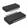
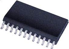
Package / Case
: SOIC-24
Features: ` Function, Pinout, and Drive Compatible
With FCT, F Logic, and AM29823
` Reduced VOH (Typically = 3.3 V) Version of
Equivalent FCT Functions
` Edge-Rate Control Circuitry for
Significantly Improved Noise
Characteristics
` Ioff Supports Partial-Power-Down Mode Operation
` Matched Rise and Fall Times
` Fully Compatible With TTL Input and
Output Logic Levels
` ESD Protection Exceeds JESD 22
2000-V Human-Body Model (A114-A)
200-V Machine Model (A115-A)
1000-V Charged-Device Model (C101)
` 64-mA Output Sink Current
32-mA Output Source Current
` High-Speed Parallel Register With
Positive-Edge-Triggered D-Type Flip-Flops
` Buffered Common Clock-Enable (EN) and
Asynchronous-Clear (CLR) InputsPinout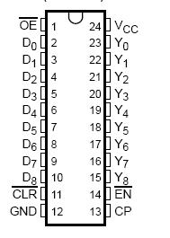 SpecificationsSupply voltage range to ground potential . . . . . . . . . . . . . . . . . . . . . . . . . . . . . . . . . . . . . . . . . . 0.5 V to 7 V
DC input voltage range . . . . . . . . . . . . . . . . . . . . . . . . . . . . . . . . . . . . . . . . . . . . . . . . . . . . . . . . .0.5 V to 7 V
DC output voltage range . . . . . . . . . . . . . . . . . . . . . . . . . . . . . . . . . . . . . . . . . . . . . . . . . . . . . . . .0.5 V to 7 V
DC output current (maximum sink current/pin) . . . . . . . . . . . . . . . . . . . . . . . . . . . . . . . . . . . . . . . . . . . 120 mA
Package thermal impedance, JA (see Note 1): P package . . . . . . . . . . . . . . . . . . . . . . . . . . . . . . . . . . . 67°C/W
Q package . . . . . . . . . . . . . . . . . . . . . . . .. . . . . . . . . . . . . . . . . . . . . . . . . . . . . . . . . . . . . . . . . . . . . . . . 61°C/W
SO package . . . . . . . . . . . . . . . . . . . . . . . . . . . . . . . . . . . . . . . . . . . . . . . . . . . . . . . . . . . . . . . . . . . . . . 46°C/W
Ambient temperature range with power applied, TA . . . . . . . . . . . . . . . . . . . . . . . . . . . . . . . . . 65°C to 135°C
Storage temperature range, Tstg . . . . . . . . . . . . . . . . . . . . . . . . . . . . . . . . . . . . . . . . . . . . . . . . 65°C to 150°C
† Stresses beyond those listed under "absolute maximum ratings" may cause permanent damage to the device. These are stress ratings only, and
functional operation of the device at these or any other conditions beyond those indicated under "recommended operating conditions" is not implied.
Exposure to absolute-maximum-rated conditions for extended periods may affect device reliability.
NOTE 1: The package thermal impedance is calculated in accordance with JESD 51.DescriptionThis bus-interface register is designed to eliminate the extra packages required to buffer existing registers and provide extra data width for wider address/data paths or buses carrying parity. The CY74FCT823T is a 9-bit-wide buffered register with clock-enable (EN) and clear (CLR) inputs, CY74FCT823T is ideal for parity bus interfacing in high-performance microprogrammed systems. This device is ideal for use as an output port requiring high IOL/IOH.
CY74FCT823T is designed for high-capacitance load drive capability, while providing low-capacitance bus loading at both inputs and outputs. Outputs are designed for low-capacitance bus loading in the high-impedance state.
CY74FCT823T is fully specified for partial-power-down applications using Ioff. The Ioff circuitry disables the outputs, preventing damaging current backflow through the device when it is powered down.
Parameters: | Technical/Catalog Information | CY74FCT823CTSOC |
| Vendor | Texas Instruments |
| Category | Integrated Circuits (ICs) |
| Mounting Type | Surface Mount |
| Package / Case | 24-SOIC (7.5mm Width) |
| Function | Master Reset |
| Number of Bits per Element | 9 |
| Number of Elements | 1 - Single |
| Current - Output High, Low | 32mA, 64mA |
| Output Type | Tri-State Non Inverted |
| Trigger Type | Positive Edge |
| Type | D-Type Bus |
| Packaging | Tube |
| Operating Temperature | -40°C ~ 85°C |
| Delay Time - Propagation | 6ns |
| Frequency - Clock | - |
| Voltage - Supply | 4.75 V ~ 5.25 V |
| Drawing Number | 296; 4040000-5; DW; 24 |
| Lead Free Status | Lead Free |
| RoHS Status | RoHS Compliant |
| Other Names | CY74FCT823CTSOC
CY74FCT823CTSOC
|
 CY74FCT823CTSOC Data Sheet