CY7C09349V

Features: • True dual-ported memory cells which allow simultaneous access of the same memory location• Two Flow-Through/Pipelined devices-4K x 18 organization (CY7C09349V)-8K x 18 organization (CY7C09359V)• Three Modes-Flow-Through-Pipelined-Burst• Pipelined output mode on ...

product image

CY7C09349V Picture
SeekIC No. : 004319698 Detail

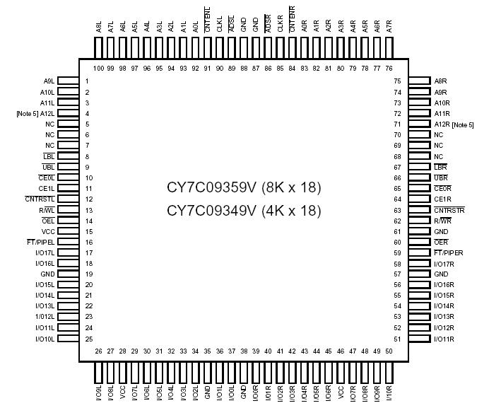
CY7C09349V: Features: • True dual-ported memory cells which allow simultaneous access of the same memory location• Two Flow-Through/Pipelined devices-4K x 18 organization (CY7C09349V)-8K x 18 organi...

floor Price/Ceiling Price

Part Number:
CY7C09349V
Supply Ability:
5000

Price Break

  • Qty
  • 1~5000
  • Unit Price
  • Negotiable
  • Processing time
  • 15 Days
Total Cost: $ 0.00

SeekIC Buyer Protection PLUS - newly updated for 2013!

  • Escrow Protection.
  • Guaranteed refunds.
  • Secure payments.
  • Learn more >>

Month Sales

268 Transactions

Rating

evaluate  (4.8 stars)

Upload time: 2024/5/6

Payment Methods

All payment methods are secure and covered by SeekIC Buyer Protection PLUS.

Notice: When you place an order, your payment is made to SeekIC and not to your seller. SeekIC only pays the seller after confirming you have received your order. We will also never share your payment details with your seller.
Product Details

Description


Features:

• True dual-ported memory cells which allow simultaneous access of the same memory location
• Two Flow-Through/Pipelined devices
-4K x 18 organization (CY7C09349V)
-8K x 18 organization (CY7C09359V)
• Three Modes
-Flow-Through
-Pipelined
-Burst
• Pipelined output mode on both ports allows fast 83-MHz operation
• 0.35-micron CMOS for optimum speed/power
• High-speed clock to data access 7.5[1, 2]/9/12 ns (max.)
• 3.3V Low operating power
-Active = 135 mA (typical)
-Standby = 10 µA (typical)
• Fully synchronous interface for easier operation
• Burst counters increment addresses internally
-Shorten cycle times
-Minimize bus noise
-Supported in Flow-Through and Pipelined modes
• Dual Chip Enables for easy depth expansion
• Upper and lower byte controls for bus matching
• Automatic power-down
• Commercial and Industrial temperature ranges
• Available in 100-pin TQFP


Pinout

  Connection Diagram


Specifications

Storage Temperature ............................ 65°C to +150°C
Ambient Temperature with
Power Applied.........................................55°C to +125°C
Supply Voltage to Ground Potential ............  0.5V to +4.6V
DC Voltage Applied to
Outputs in High Z State ..........................0.5V to VCC+0.5V
DC Input Voltage................................... .0.5V to VCC+0.5V
Output Current into Outputs (LOW) ........................... 20 mA
Static Discharge Voltage .......................................... >2001V
Latch-Up Current..................................................... >200 mA


Description

The CY7C09349V and CY7C09359V are high-speed 3.3V synchronous CMOS 4K and 8K x 18 dual-port static RAMs. Two ports of CY7C09349V  are provided, permitting independent, simultaneous access for reads and writes to any location in memory.[4] Registers on control, address, and data lines allow for minimal setup and hold times. In pipelined output mode, data is registered for decreased cycle time. Clock to data valid tCD2 = 7.5 ns (pipelined). Flow-through mode can also be used to bypass the pipelined output register to eliminate access latency. In flow-through mode data will be available tCD1 = 18 ns after the address is clocked into the device. Pipelined output or flowthrough mode is selected via the FT/Pipe pin.

Each port of CY7C09349V contains a burst counter on the input address register. The internal write pulse width is independent of the LOWto- HIGH transition of the clock signal. The internal write pulse is self-timed to allow the shortest possible cycle times.

A HIGH on CE0 or LOW on CE1 for one clock cycle will power down the internal circuitry to reduce the static power consumption. The use of multiple Chip Enables allows easier banking of multiple chips for depth expansion configurations. In the pipelined mode, one cycle is required with CE0 LOW and CE1 HIGH to reactivate the outputs.

Counter CY7C09349V enable inputs are provided to stall the operation of the address input and utilize the internal address generated by the internal counter for fast interleaved memory applications. A port's burst counter is loaded with the port's Address Strobe (ADS). When the port's Count Enable (CNTEN) is asserted, the address counter will increment on each LOW-to-HIGH transition of that port's clock signal. CY7C09349V will read/write one word from/into each successive address location until CNTEN is deasserted. The counter CY7C09349V  can address the entire memory array and will loop back to the start. Counter Reset (CNTRST) is used to reset the burst counter.

All parts are available in 100-pin Thin Quad Plastic Flatpack (TQFP) packages.


Customers Who Bought This Item Also Bought

Margin,quality,low-cost products with low minimum orders. Secure your online payments with SeekIC Buyer Protection.
Inductors, Coils, Chokes
Undefined Category
Motors, Solenoids, Driver Boards/Modules
Memory Cards, Modules
View more