Features: •128K X 32 common I/O
•3.3V 5% and +10% core power supply (VDD)
•2.5V or 3.3V I/O supply (VDDQ)
•Fast clock-to-output times
-6.5 ns (133-MHz version)
-7.5 ns (117-MHz version)
-8.0 ns (100-MHz version)
•Provide high-performance 2-1-1-1 access rate
•User-selectable burst counter supporting Intel®Pentium® interleaved or linear burst sequences
•Separate processor and controller address strobes
•Synchronous self-timed write
•Asynchronous output enable
•Lead-Free 100-pin TQFP and 119-ball BGA packages
•"ZZ" Sleep Mode optionPinout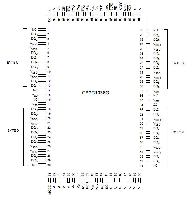 Specifications(Above which the useful life may be impaired. For user guide-lines, not tested.)
Storage Temperature .............................65°C to +150°C
Ambient Temperature with
Power Applied.........................................55°C to +125°C
Supply Voltage on VDD Relative to GND........0.5V to +4.6V
DC Voltage Applied to Outputs
in tri-state..........................................0.5V to VDDQ + 0.5V
DC Input Voltage..................................0.5V to VDD + 0.5V
Current into Outputs (LOW).........................................20 mA
Static Discharge Voltage........................................... >2001V
(per MIL-STD-883, Method 3015)
Latch-up Current..................................................... >200 mA DescriptionThe CY7C1338G is a 131,072 x 32 synchronous cache RAM designed to interface with high-speed microprocessors with minimum glue logic. Maximum a ccess delay from clock rise is 6.5 ns (133-MHz version). A 2-bit on-chip counter captures the first address in a burst and increments the address automati- cally for the rest of the burst access. All synchronous inputs of CY7C1338G are gated by registers controlled by a positive-edge-triggered Clock Input (CLK). The synchronous inputs of CY7C1338G include all addresses, all data inputs, address-pipelining Chip Enable(CE1</a>), depth-expansion Chip Enables (CE2</a> and CE3</a>), Burst Control inputs (ADSC</a>, ADSP</a>, and ADV</a>), Write Enables(BW</a>[A:D], and BWE</a>), and Global Write (GW</a>). Asynchronousinputs include the Output Enable (OE</a>) and the ZZ pin.
The CY7C1338G allows either interleaved or linear burst sequences, selected by the MODE input pin. A HIGH selects an interleaved burst sequence, while a LOW selects a linear burst sequence. Burst accesses CY7C1338G can be initiated with the Processor Address Strobe (ADSP</a>) or the cache Controller Address Strobe (ADSC</a>) inputs. Address advancement is controlled by the Address Advancement (ADV</a>) input.
Addresses and chip of CY7C1338G enables are registered at rising edge of clock when either Address Strobe Processor (ADSP</a>) or Address Strobe Controller(ADSC</a>) are active. Subsequent burst addresses can be internally generated as controlled by the Advance pin (ADV</a>).
The CY7C1338G operates from a +3.3V core power supply while all outputs may operate with either a +2.5 or +3.3V supply. All inputs and outputs are JEDEC-standard JESD8-5-compatible.

 CY7C1338G Data Sheet


