Features: • 128K * 36 common I/O
• 3.3V 5% and +10% core power supply (VDD)
• 2.5V or 3.3V I/O supply (VDDQ)
• Fast clock-to-output times
- 6.5 ns (133-MHz version)
- 7.5 ns (117-MHz version)
- 8.0 ns (100-MHz version)
- 11.0 ns (66-MHz version)
• Provide high-performance 2-1-1-1 access rate
• User-selectable burst counter supporting Intel®Pentium®interleaved or linear burst sequences
• Separate processor and controller address strobes
• Synchronous self-timed write
• Asynchronous output enable
• Offered in JEDEC-standard 100-pin TQFP and 119-ballBGA packages
• "ZZ" Sleep Mode option
Pinout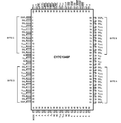 Specifications
(Above which the useful life may be impaired. For user guidelines,not tested.)
Storage Temperature .................................65 to +150
Ambient Temperature with
Power Applied.............................................55 to +125
Supply Voltage on VDD Relative to GND........0.5V to +4.6V
DC Voltage Applied to Outputs
in three-state .....................................0.5V to VDDQ+ 0.5V
DC Input Voltage..................................0.5V to VDD + 0.5V
Current into Outputs (LOW)....................................... 20 mA
Static Discharge Voltage...........................................>2001V
(per MIL-STD-883, Method 3015)
Latch-up Current..................................................... >200 mA
DescriptionThe CY7C1345F is a 131,072 x 36 synchronous cache RAMdesigned to interface with high-speed microprocessors withminimum glue logic. Maximum access delay from clock rise is6.5 ns (133-MHz version). A 2-bit on-chip counter captures thefirst address in a burst and increments the address automaticallyfor the rest of the burst access. All synchronous inputs of CY7C1345F are gated by registers controlled by a positive-edge-triggeredClock Input (CLK). The synchronous inputs of CY7C1345F include alladdresses, all data inputs, address-pipelining Chip Enable(CE1), depth-expansion Chip Enables (CE2 and CE3), BurstControl inputs (ADSC , ADSP , and ADV ), Write Enables(BW[A:D],and BWE ), and Global Write (GW). Asynchronousinputs include the Output Enable (OE) and the ZZ pin.
The CY7C1345F allows either interleaved or linear burstsequences, selected by the MODE input pin. A HIGH selectsan interleaved burst sequence, while a LOW selects a linearburst sequence. Burst accesses can be initiated with the
Processor Address Strobe (ADSP) or the cache ControllerAddress Strobe (ADSC ) inputs.
Addresses and chip CY7C1345F enables are registered at rising edge ofclock when either Address Strobe Processor (ADSP ) or Address Strobe Controller (ADSC ) are active. Subsequentburst addresses can be internally generated as controlled bythe Advance pin (ADV ).
The CY7C1345F operates from a +3.3V core power supplywhile all outputs may operate with either a +2.5 or +3.3Vsupply. All inputs and outputs are JEDEC-standardJESD8-5-compatible.

 CY7C1345F Data Sheet


